The schematic diagram only indicates the electrical connection relationship between components, and does not represent the actual connection. Therefore, we need to layout these connection relationships in the actual PCB board. That is to say, when drawing the schematic diagram, you do not have to consider the layout, wiring, EMC and other various issues, as long as the components and components are connected.
Take Altium designer as an example
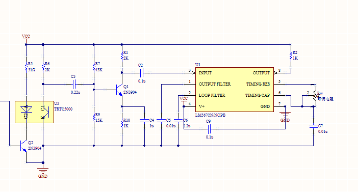
This is a schematic diagram drawn by Altium designer
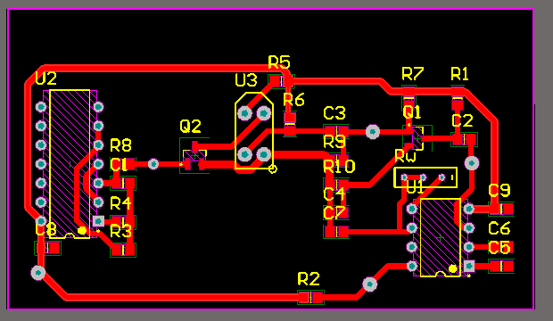
Schematic diagram is used to show the principle of the circuit, with some symbols to replace the real components, used for PCB designers to see.The figure below is the PCB drawing designed according to the schematic diagram, which is
PCB layout.
Layout is the arrangement of real electronic components on the printed circuit board, which is used to produce PCB.