High-frequency boards, e.g. for wireless applications and data rates in the upper GHz range have special demands on the material used:
Homogeneous construction with low tolerances in insulation thickness and dielectric constant
For many applications, it is sufficient to use FR4 material with an appropriate layer buildup. In addition, we process high-frequency materials with improved dielectric properties. These have a very low loss factor, a low dielectric constant, and are primarily temperature and frequency independent.
Additional favourable properties are high glass transition temperature, an excellent thermal durability, and very low hydrophilic rate.
We use (among others) Rogers or PTFE materials (for example, Teflon from DuPont) for impedance controlled high frequency circuit boards. Sandwich buildups for material combinations are also possible.
One thing that really needs special attention is the denouement.The fundamental concepts do not change when going from low to high frequencies.But implementation may require some improvement.
simply because low frequency circuits will often be fully functional when decoupling is suboptimal or,to put it mildly,rather average quality. In other words,low-frequency circuits are quite forgiving when it comes to decoupling techniques.And therefore, we may have developed design habits that are not really suitable for High Frequency PCB.
The problem is this:In the context of digital circuits,bypass capacitors store charge and release that charge to the chip to compensate for the transient noise generated by the switching action of semiconductor components.
At low operating frequencies,the capacitor has enough time to discharge and then recharge before the IC needs another surge in current. However,as the frequency increases,the board designer must try to reduce parasitic resistance.
One of the most important points when working with High Frequency PCB is the return current.Interestingly,many engineers when designing PCBs,forget it or simply never thought or guessed it.
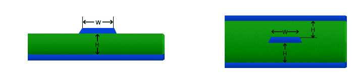
A microstrip is a transmission line in the TOP or BOTTOM layer and has only one plane as a reference;
A stripline is a transmission line in an inner layer of the PCB and it has a plane above and a plane below it as reference.
Therefore,using the theory of electrical networks in the distributed model of transmission line and with a reference plane we have to:
For High Frequency PCB, usually above 100 [Khz], the impedance is dominated by the line inductance, that is, the loop that the forward current makes with the return current.Thus,the higher the frequency,the return current will be concentrated further below the flow current,where the loop and impedance are lower
With the advent of the 5G communication era, the requirements for communication boards are more high-frequency and higher-speed. So, the processing requirements for High Frequency PCB circuit boards are also higher.
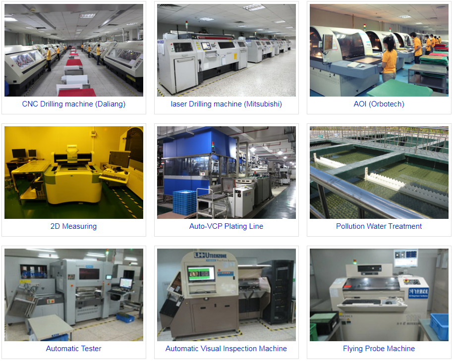
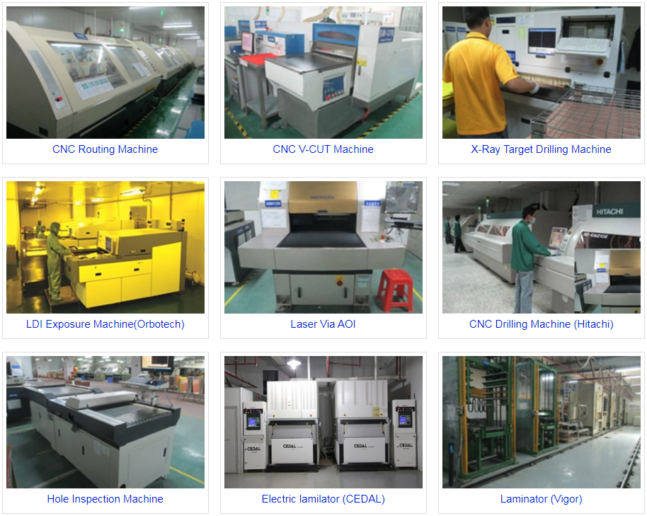
For many years,High Frequency PCB manufacturers have been focusing on high frequency PCB circuit board processing, mastering high-level copper-filled electroplating technology.Professional High Frequency PCB manufacturing companies can provide high- frequency multilayer PCB circuit boards with:
High quality
High stability and
Best adaptability .
High Frequency PCB Printing Methods
Transferring the designed printed circuit board on the printed circuit board (copper pertinax) is the most important step in the production of the printed circuit board and requires special attention.
There are many methods used in printing the printed circuit board. The designer chooses the desired method according to his needs and possibilities. In this section, commonly used card making methods will be explained to you. These methods;
Masking Method
The pencil method by drawing on the card
Positive-20 (Photo-Resist) Method
Prepaid Card Technique
Screen Printing Method
PnP Method
The Operating Frequencies of High Frequency PCB
High-frequency printed circuit boards are technologically unique models of dielectrics with operating frequencies from several MHz to tens of GHz. Feature: they are used to equip high-frequency equipment even in cases where the use of traditional FR4 glass fabric materials is impossible.
The most important parameters of high-frequency printed circuit boards
Dielectric constant: 2.2-10.2 GHz.
Signal delay characteristics.
Thickness criteria: 0.2-8 mm.
Type of foil-clad material.
Dielectric loss tangents: 0.0009-0.004.
Materials
Manufacturers use special low dielectric constant (<3 F) laminates to create high frequency PCBs. They have a stable, wide frequency range and insignificant dielectric losses. Such materials are manufactured by Neltech, Taconic and Rogers and others.
We list the most popular microwave laminates:
Reinforced PTFE type – ULTRALAM 2000.
Ceramic – RT / duroid 6000.
Thermostable, made on the basis of hydrocarbon ceramics – TMM.
Features of High-frequency Printed Circuit Boards Production
High-frequency printed circuit boards are created on the basis of fluoroplastics in several ways: positive combination and tenting method. Note that the main significant difference between these methods is the presence of the stage of applying a metal resist to a copper surface (combined positive method). In turn, the production of high-frequency printed circuit boards by the tenting method greatly simplifies the production process, reducing time and money.
The main feature: when creating multi-layer high-frequency dielectrics, laminates are used only as outer layers, while the inner ones are filled with standard epoxy glass cloth materials.
TOP 10 Tips for Designing High Frequency PCBs
More recently, the word “high frequency” did not exist in the vocabulary of PCB designers. But now, it seems, everything has turned upside down.
In the past, it was all about putting all the pieces of the puzzle together and thinking through the signal path by designing the PCB layout. What are the differences in the design of high frequency printed circuit boards? There are many invisible forces to worry about, such as electromagnetic interference, mutual interference, signal reflections, and the list goes on. In this article, we offer you some practical tips to help you succeed in designing your first RF PCB.
More data, more electromagnetic interference
In 2005, 3 Gbps was considered typical of high-speed data transmission, but today engineers are dealing with 10 Gbps and even 25 Gbps. And this is done not only because we strive to achieve higher clock speeds, but also because we strive to reduce the size of devices to keep up with the growing demands of consumers. Whatever device you design today , chances are you already included various nodes operating at high speeds, be it DDR, PCI Express, USB, SATA, etc.
The main concern in the design of high frequency printed circuit boards is to eliminate interference. The higher the baud rate, the more difficult it becomes to maintain the integrity of your signals. Most of these problems are related to the emission of electromagnetic waves. This radiation is relatively harmless with weak interactions with electrical circuitry.
However, when it begins to interfere with the operation of your electronic device as a whole, the radiation turns into interference, opening up a new world of tasks for you to solve. If you’ve ever heard of or encountered noise related problems, then you know exactly what we’re talking about.
Any current creates a magnetic field. This is how the spread of electromagnetic radiation begins.
So, you might be wondering how you even know that you are working on a high frequency project, if it does not reveal problems with electromagnetic radiation. There are several scientific theories, but we will narrow them down to the 3 most popular:
Frequency.The first theory is that high frequency design is such because of the operating frequency of the PCB and its ability to influence the performance of the electronic circuit. Some believe that this threshold starts at 50 MHz. Others divide device speeds into groups: low-frequency (<25 MHz), medium-frequency (25-100 MHz), high-frequency (100-1000 MHz), and above – ultra-high frequency, which are the designers of radio transmitting devices.
Conductive tracks. There is a theory that it is possible to use the physical dimensions of the conductive paths to determine the high frequency of the device. Its guiding principle is that if the signal travel time on the track is more than 1/3 of the switching time of the device signal, then you are dealing with a high frequency device.
Modularity.The latter point of view takes a general approach that looks at circuit design as a whole and asks the next question – is your system physically operating as a single system? Or do you have a set of subcircuits, from which one large circuit is assembled, in which individual modules work independently? In the latter case, you are dealing with the realm of high frequency devices.
So, you have determined that your future project is high frequency. Great. Now let’s take a look at all the possible “background noises” that you have to deal with. Let’s take a closer look at the top 10 tips for success in device design.
# 1 – Always Start Designing Your RF Device with Planning
We’ll start with the most obvious advice, but there is a reason for that. Without a plan and strategy for creating your high frequency project, you are likely to run into delays, confusion and unexpected problems. So before you draw a single symbol or make a single connection, you need to create a kind of checklist. Here are a number of questions to ask yourself first:
System Organization– Do I have a visual diagram to help me visualize the interconnections of all my subcircuits and the reliable return flow?
Signal Rate– Do I know the maximum frequency and fastest switching rate for each of my signals?
Power Supply– Does the documentation cover every voltage and wattage requirement to power all of my ICs, and do I need to separate the power layers?
Sensitive Signals– Do I have a plan for meeting differential signal requirements, impedance matching and track length, or signal propagation?
This is not a complete list of questions to answer yourself during the planning phase, but it will serve as a good starting point. You will most likely need to work with the manufacturer of your device to determine its minimum tolerance requirements. And you also need to agree on a development strategy to reduce the noise level of your high frequency signals using a variety of tracing methods, including microstrip transmission lines or stripline traces.
# 2 – Document Every Detail of Every Layer of Your Board for Further Production
To create the plan described in tip # 1, it’s time to define and carefully document the layer requirements for your board. This is the ideal time to interact with the manufacturer to select the material for your board and determine the constraints that need to be placed in the design code. Since we are talking about materials, most likely you will be working with one of the following materials:
FR-4 is great material when running at <5Gbps clock rates. It is considered a low speed material. FR-4 allows you to set the impedance quite accurately , it is also widely known for its low cost.
Nelco, SIor Megtron – In the realm of high frequency devices, chances are you will be working with these materials. Each of them is suitable for operating at 5-25 Gbps clock rates.
Rogers– If your first high-frequency device is running at over 56 Gbps, chances are you will end up with Rogers layered material. This material is capable of operating at high frequencies and at high temperatures, it is known for its high impedance uniformity, but it is also expensive to manufacture.
Once you have selected the material you need to make your board, it’s time to decide on other strategies for forming your board layers.
First, you should always have a Signal layer adjacent to a Plane to give your signals an efficient return path.
It is also worth placing all high speed signal circuits on the inner layers between the Plane layers to provide shielding from all external sources of electromagnetic radiation.
Finally, multiple ground layers should be considered in the PCB layer set. This will help lower the nominal impedance and reduce common-mode emissions affecting your circuit.
# 3 – Layout – Break Your Board into Logical Chunks
Along with planning your high speed device design requirements and layer assignments, you also need to decide how your PCB will be organized. Remember we said above that high frequency devices are a set of subcircuits? You need to decide how these subcircuits will be located on the common board.
This is especially true for digital and analog modules, which must be carefully isolated from each other to reduce any potential interference. When planning the physical layout of your board, use something like the diagram shown in the figure below. The engineer who designed this board clearly separated the digital and analog circuits, and also isolated the power module from both the digital and analog modules.
# 4 – Determine Using Power and Ground Layers
Now that the subcircuit locations and layer configurations have been fully defined, it’s time to pay attention to the smallest details that need to be clarified during the design of the board . First, this is the ground plane, which must be solid. By this we mean that the ground plane should not be broken by any signal tracks. If you break this layer, signals will have to look for workarounds, which can lead to nasty EMI and signal delays. If you do need to break the ground plane, remember to install a 0 ohm resistor along the signal path to make it easier for the return signal to find its path.
# 5 – The Size of the Contact Pads should be Made as Small as Possible
Any PCB designs you have worked on in the past may have larger pads than necessary. This was done for obvious reasons. This makes it easier to apply solder to the pad, to control them faster, and the accuracy of the placement of board components is not so important.
However, in the design of high-frequency printed circuit boards, the value of every millimeter of surface skyrockets – every millimeter you save will come in handy. In light of this, we recommend observing the minimum allowances for all pads at the level of 0-5% of the dimensions of the leads of the parts to be installed. Compare this to the traditional 30% allowance for conventional electronic devices.
Why save space? This will not only help us improve mechanical strength, but it will also allow us to reduce parasitic capacitances, which play a significant role when it comes to high frequencies. More importantly, the less space you set aside for pads, the more room you have for differential pairs of conductors, vias, and high-density parts such as FPGAs and integrated circuits.
# 6 – Route Signals for Maximum Shielding
High frequency signals on your board create a mass of electromagnetic radiation as they travel from source to consumer. The last thing you would like to get is for the two signals to cause mutual interference with each other or affect adjacent parts. To avoid this, route the signal traces for maximum shielding, following the guidelines below:
Long parallel signal paths should be kept as short as possible to avoid signal interference or crosstalk.
The distance between the signal paths should be as great as possible, and even they should be placed on different layers, especially if strong interference is expected from them.
When routing signal paths on different layers, make sure they are at right angles to each other. Thus, if the tracks run horizontally on one signal layer, then on the other they should run vertically, at an angle of 45 degrees, etc.
# 7 – Provide an Efficient Return Current Path
In high-speed board designs, each of the signals tries to find a path from source to consumer with the lowest impedance. For clocks and other high-speed I / O devices, the goal of providing the shortest path may require the use of vias. Without them, you can run into currents around discontinuities in the ground plane, resulting in loss of signal integrity.
# 8 – Use the 3W Rule to Minimize Communication between Tracks
Interconnected transmission lines can play a bad role in maintaining the integrity of the signal during transmission. To minimize this risk, there is an obligatory general rule to separate the tracks from each other as far as possible, although this rule is difficult to follow when designing a real board.
If you’ve ever wondered how far apart the tracks should be to minimize communication between them, then use the 3W rule. It states that the distance between the tracks, measured between the longitudinal axes of the tracks, must be three times greater than the width of the individual track. You can also increase the distance from 3x to 10x to get much less signal from one track on the signal of another track and to reduce crosstalk.
# 9 – Use the 20H Rule to Minimize Communication Between Layers
In addition to the risk of signal interconnection between individual tracks, you should also think about the connection between the power and ground layers of the board. When such a connection occurs, radiation in the radio frequency range, called fringing, begins to break off the edges of the board.
To prevent this phenomenon, make the power layer smaller than the adjacent ground layer. This will allow the edge flux to be absorbed by the grounding layer instead of emitting it into the external environment. However, how much smaller should the nutritional layer be? Use the 20H rule, which says that the power layer should be less than 20 times the dielectric thickness between adjacent power and ground layers.
# 10 – In conclusion – General Rules for Tracing a Printed Circuit Board
In conclusion of our TOP-10 tips, we will mention board routing, which in itself deserves a separate article, and possibly a book, which would talk about such things as radiation in the radio frequency range, microwaves, and antenna design. This list is not exclusive, so be sure to ask an experienced PCB routing engineer for help with tasks like yours. So:
Do not use 90-degree bends in the tracks. First, avoid using 90-degree track curvature. Tracks bent at right angles can cause signal reflections.
Differential pairs. You can get mutual suppression of electromagnetic fields if both signal lines in your differential pair have the same length and a constant distance between them. This will most likely require adjusting the track lengths in your PCB design application.
Transmission lines. Take the time to carefully design transmission lines using microstrip lines and strip lanes. Microstrip lines use only one support layer separated by a dielectric. If you need better shielding, use a strip transmission line between multiple ground layers and dielectric layers.
New Solutions in the Design of High-frequency Devices
When working on your first RF PCB design project, you are likely to run into new, previously unknown problems. They will no longer be just about putting all the puzzle pieces together. Now you need to think about how exactly the signals behave when passing along the tracks, and how they affect all the details of the PCB. And at the end of the day, it all boils down to EMI problems.
As you dive deeper into the world of high-speed devices, you will gain new strategies and knowledge for dealing with electromagnetic interference while maintaining EMC or EMC. So use these TOP 10 tips to get started on your first project. However, there is still much to be learned!
Special materials are required to achieve the high frequency provided by this type of printed circuit board - any changes in the Er value of these materials can affect the impedance of the board. Many PCB designers turn to
dielectric material for its lower dielectric loss, reduced signal loss, lower cost of circuit fabrication and better suitability for fast-turnaround prototyping applications.
Apart from choosing the appropriate PCB material and determining the correct the value of the Er, designers should take parameter such as conductor width and spacing, substrate constant into consideration. These parameters must be exactly specified and implemented with the highest level of process control.
who make all our efforts to meet Your Needs.
We're an experienced full service PCB manufacturer who provides a reliable, superior-performing high-frequency PCB fabrication services.
We manufacture high-frequency PCBs with frequency typically in the range from 500MHz to 2GHz.
For High Frequency PCB manufacturing price, please send your PCB file (Gerber format preferred | Preorder Checklist) & requirements using the contact form below, we'll quote at quickest speed.
Want to know our customizable high frequency PCB solution? Not sure which PCB material is the best choice for your project? Need advanced specifications not listed in the table above? Contact our engineers to get a practical solution.
Many RF applications are multi-layer affairs and the properties of the board can be fine-tuned by mixing and matching different materials to strengthen the balance of electrical performance, thermal properties and cost.
Composite boards, often referred to as hybrid multi-layer PCBs, can be difficult to build because many layer-to-layer interactions must be taken into account for multiple steps along the PCB manufacturing process. Additional challenges also arise, such as a mixed-signal PCB design that combines analogue and digital components, generating a list of variables that becomes quite large. With so many current applications and emerging markets for RF, the future is bright indeed.
However, RF boards are clearly complex and have many variables that must be addressed and exhibit unusual behavior that is not shared with their lower-frequency cousins. While it may be challenging, it’s not “black magic.”
If you are seeking to manufacture RF PCBs and have questions relating to manufacturing or need a quote, PCBSky, as a professional
, is always here to help you with our extensive engineering expertise.

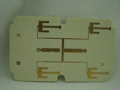 Rogers PCB
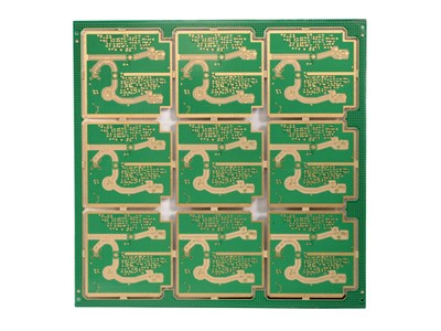 Hybrid PCBs
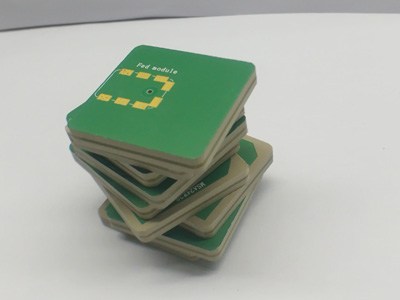 PTFE Teflon PCB