PCB manufacturing has evolved significantly in recent years, with one of the key advancements being the widespread adoption of Via in Pad (VIP) technology. In modern electronics design and manufacturing, VIP has emerged as a critical factor for enhancing PCB performance and reliability. However, the successful implementation of Via in Pad technology requires rigorous manufacturing processes and quality control measures to ensure that printed circuit boards operate flawlessly under diverse environmental conditions.
This article delves deep into the pivotal role of Via in Pad technology in PCB manufacturing, discussing best practices and essential quality control considerations to ensure the production of high-quality PCBs. Whether you’re an electrical engineer, a PCB designer, or a manufacturer, gaining insights into Via in Pad technology is paramount, as it can significantly impact the quality and functionality of electronic devices.
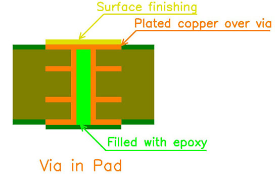
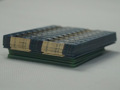
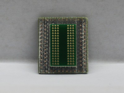
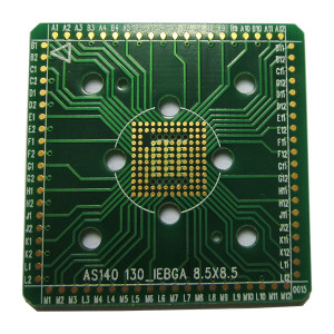
Via in Pad, as the name suggests, involves placing a via (a plated through-hole) directly within or under the surface mount component’s solder pad on a PCB. This technique is employed primarily to save space and reduce the overall footprint of components on the board, a crucial aspect in the design of modern, compact electronic devices.
However, while Via in Pad offers numerous advantages, such as increased component density and shorter trace lengths, it also presents specific challenges. These include soldering complexities during assembly and potential reliability concerns. To navigate these challenges effectively, it’s essential to have a comprehensive understanding of the technology and its associated nuances.
In this article, we’ll explore the benefits and challenges of Via in Pad technology, discuss the latest trends in its application, and provide practical insights into ensuring the reliability and performance of PCBs manufactured using this advanced technique. Let’s begin by examining the advantages of Via in Pad technology in detail.
Via in Pad technology offers several compelling advantages that make it a preferred choice in modern PCB design and manufacturing:
By placing vias within the solder pads, designers can maximize the use of available PCB real estate. This means more components can be placed in a smaller space, a crucial consideration in miniaturized electronics where every millimeter counts.
The proximity of vias to components allows for shorter trace lengths, which translates to reduced signal travel times. This reduction in trace length can help improve signal integrity and reduce the risk of signal degradation or interference.
Vias in Pad can also act as effective heat sinks. This property is especially valuable in dissipating heat generated by power components, ensuring that the PCB operates within safe temperature limits.
With shorter trace lengths, controlled impedance, and reduced parasitic capacitance and inductance, Via in Pad technology can lead to better signal integrity. This is crucial for high-speed digital signals and analog circuits where signal quality is paramount.
Perhaps one of the most significant advantages is the space-saving aspect. As electronic devices continue to shrink in size while increasing in complexity, Via in Pad technology helps designers meet the demands for smaller, more powerful devices without compromising functionality.
In the subsequent sections of this article, we will delve deeper into the challenges associated with Via in Pad technology, discuss how to mitigate these issues during manufacturing, and explore real-world applications and success stories. By the end, you will have a comprehensive understanding of Via in Pad technology and be better equipped to leverage its advantages while overcoming its challenges in your PCB manufacturing endeavors.
While Via in Pad technology offers significant advantages, it also introduces specific challenges that require careful consideration and mitigation:
Soldering components with vias in their pads can be more complex than traditional surface mount technology. During assembly, there’s a risk of solder wicking into the via, potentially leading to solder voids, incomplete connections, or other soldering defects. Controlling the soldering process becomes paramount.
The process of creating vias in pads adds complexity and cost to the manufacturing process. Specialized equipment and techniques may be required for drilling and plating vias within the solder pads, which can increase production expenses.
Ensuring the reliability of Via in Pad technology is essential. Poor soldering or design choices can lead to issues such as solder joint cracking, delamination, or reduced thermal performance. These problems can affect the long-term reliability and functionality of the PCB.
Designing PCBs with Via in Pad technology demands attention to detail. Careful placement of vias, consideration of signal and power integrity, and adherence to industry standards are critical to achieving optimal results.
Via in Pad technology can affect controlled impedance requirements, particularly in high-frequency applications. Engineers must carefully calculate and control impedance to maintain signal integrity.
In the sections that follow, we will explore how to address these challenges effectively. We’ll provide insights into manufacturing techniques, quality control measures, and design principles that can help you harness the benefits of Via in Pad technology while ensuring the reliability and performance of your PCBs.
Whether you’re a seasoned PCB designer looking to expand your knowledge or a manufacturer seeking to optimize your production processes, this article aims to equip you with the expertise needed to navigate the intricacies of Via in Pad technology successfully. Let’s begin with a closer look at the manufacturing aspects of Via in Pad PCBs.
Manufacturing Via in Pad PCBs requires a thorough understanding of the technology and meticulous attention to the production process. Here are some key considerations and best practices for successful Via in Pad manufacturing:
By adhering to these manufacturing practices and quality control measures, you can mitigate the challenges associated with Via in Pad technology. This will ultimately result in the production of high-quality PCBs that meet the demands of today’s electronics industry.
In the subsequent sections of this article, we will explore real-world applications and case studies showcasing the successful implementation of Via in Pad technology. These examples will illustrate how this advanced technique has been leveraged to create innovative electronic devices across various industries.
To gain a deeper appreciation for the practical benefits of Via in Pad technology, let’s explore some real-world applications and success stories that highlight its versatility and impact:
These examples demonstrate the broad spectrum of applications where Via in Pad technology is making a difference. Whether it’s enhancing the functionality of consumer electronics, improving the reliability of life-saving medical devices, or enabling space exploration, Via in Pad has become an indispensable tool in modern electronics design and manufacturing.
The adoption of Via in Pad technology continues to grow as the electronics industry strives for smaller, more efficient, and higher-performing devices. By understanding the advantages, challenges, and best practices associated with this technology, engineers, designers, and manufacturers can harness its full potential, ensuring the successful development of cutting-edge electronic products that meet the evolving demands of our technologically-driven world.
As we conclude our exploration of Via in Pad technology, it’s evident that this advanced technique has become a linchpin in the ever-evolving landscape of electronic design and manufacturing. Its ability to enhance component density, signal integrity, and thermal management while saving precious space on PCBs has made it an indispensable tool for engineers and designers.
However, the journey of Via in Pad technology is far from over. The future holds exciting developments and trends in this field:
In this dynamic landscape, staying informed about the latest developments and trends in Via in Pad technology will be essential for engineers, designers, and manufacturers alike. By embracing innovation and adapting to emerging challenges, the electronics industry will continue to deliver cutting-edge solutions that shape the future of technology.
Via in Pad technology is not just a technological advancement; it’s a catalyst for innovation across various industries. Its ability to optimize space, enhance performance, and ensure reliability positions it as a critical component in the ongoing evolution of electronic devices. As we move forward, the possibilities and opportunities enabled by Via in Pad technology are limited only by our creativity and commitment to pushing the boundaries of what’s possible in electronics.
The advantage of the resin plug hole relative to the solder resist plug hole is that the flatness of the pad of the resin plug hole is higher than the flatness of the hole of the solder resist plug, and the disadvantage is high cost and complicated process.
Via in Pad: Filled with epoxy; Surface Finishing; Plated Copper Over Via.