Choosing the best High-Density Interconnect (HDI) PCB supplier is crucial for the performance of electronic products. In a highly competitive market, the quality of circuit boards directly impacts product reliability and performance. This article will guide you on making informed supplier choices.
HDI PCBs have become a vital component of modern electronic devices, enabling smaller, lighter, and more powerful equipment. To harness the full potential of HDI PCBs, selecting an experienced and reputable supplier is paramount.
PCBSky will delve into how to evaluate potential HDI PCB suppliers to ensure they meet your project requirements and contribute to the success of your product. Whether you are a startup or a large manufacturer, this article will provide key insights into choosing the best HDI PCB supplier.
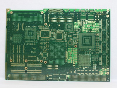
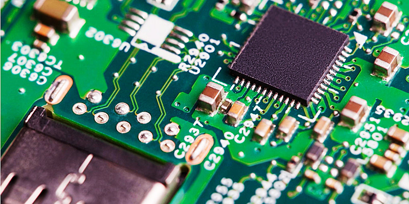
High-Density Interconnect (HDI) printed circuit boards have revolutionized the world of electronics. These compact and technologically advanced circuit boards play a pivotal role in enabling the creation of smaller, lighter, and more powerful electronic devices. The significance of HDI PCBs lies in their ability to pack more components into a smaller space, leading to increased functionality and performance.
Traditional printed circuit boards (PCBs) often face limitations when it comes to miniaturization. However, HDI technology overcomes these constraints by employing multiple layers of fine lines and vias, allowing for intricate and densely packed designs. This means that in a world where consumers and industries demand ever-smaller electronic devices, HDI PCBs are essential for meeting these requirements.
HDI PCBs are commonly found in smartphones, tablets, laptops, medical devices, and automotive electronics, among other applications. In these devices, HDI technology not only saves space but also enhances signal integrity and reduces electromagnetic interference. This results in more reliable and efficient electronic systems.
As technology continues to advance, the demand for HDI PCBs will only increase. The significance of these boards goes beyond size reduction; it extends to improving the overall performance, reliability, and functionality of electronic products. Therefore, understanding the importance of HDI PCBs is fundamental for both manufacturers and consumers in today’s fast-paced world of electronics.
High-Density Interconnect (HDI) printed circuit board technology offers a host of advantages that are driving its widespread adoption in the electronics industry. These advantages are at the core of what makes HDI PCBs indispensable for modern electronic devices.
One of the primary benefits of HDI PCB technology is its ability to support miniaturization. With more components and connections packed into a smaller space, electronic devices can be made smaller and more lightweight. This is especially critical for applications like smartphones, where slim and lightweight designs are highly sought after.
Additionally, HDI PCBs excel in enhancing electrical performance. The use of fine lines and vias allows for shorter signal paths and reduced electromagnetic interference, resulting in improved signal integrity. This leads to faster data transmission, lower power consumption, and overall better performance.
Moreover, the higher component density achievable with HDI technology enables greater design flexibility. Designers can create complex and highly integrated circuits, which can lead to innovative product features and functionalities.
Another advantage is improved reliability. HDI PCBs are designed with tighter tolerances and undergo rigorous quality control measures, making them less prone to defects. This translates to longer product lifecycles and reduced maintenance costs.
Furthermore, HDI PCBs are often more cost-effective in terms of material usage and manufacturing efficiency. While the technology itself may have a higher initial setup cost, the overall savings in terms of reduced material waste and improved production yield make it a smart investment.
In conclusion, the key advantages of HDI PCB technology, including miniaturization, enhanced electrical performance, design flexibility, improved reliability, and cost-effectiveness, make it a crucial component in the development of advanced electronic devices. As technology continues to evolve, these advantages will continue to drive the adoption of HDI PCBs across various industries.
1 Consumer Electronics: HDI PCBs are widely used in consumer electronics such as smartphones, tablets, wearables, and IoT devices. The demand for smaller, lightweight, and feature-rich devices has driven the adoption of HDI PCBs to accommodate the increasing complexity of electronic components while maintaining a compact form factor.
2 Medical Devices: The medical industry relies on HDI PCBs for a wide range of applications, including diagnostic equipment, patient monitoring devices, and implantable medical devices. The compact size and high-density interconnects of HDI PCBs enable the development of advanced medical technologies that are portable, precise, and reliable.
3 Automotive Electronics: With the growing complexity of automotive electronics, HDI PCBs play a vital role in automotive applications. They are used in advanced driver-assistance systems (ADAS), infotainment systems, and engine control units (ECUs). HDI PCBs provide the necessary space-saving and high-performance capabilities required for modern automotive designs.

Selecting the right High-Density Interconnect (HDI) PCB supplier is a critical decision that can profoundly impact the success of your electronic project. To make an informed choice, it’s essential to consider several key criteria:
Experience and Expertise: Look for a supplier with a solid track record in manufacturing HDI PCBs. Experience is often a strong indicator of a supplier’s ability to meet your specific requirements and navigate complex design challenges.
Reputation and References: Investigate the supplier’s reputation within the industry. Seek out customer reviews and testimonials, and ask for references from past clients to gauge their level of satisfaction.
Quality Control Standards: Assess the supplier’s commitment to quality control. Inquire about their quality control processes, certifications (e.g., ISO 9001), and testing procedures to ensure consistent and reliable PCB production.
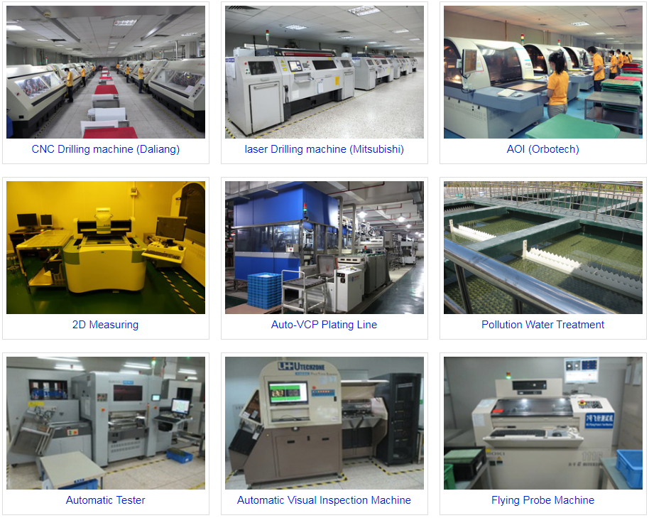
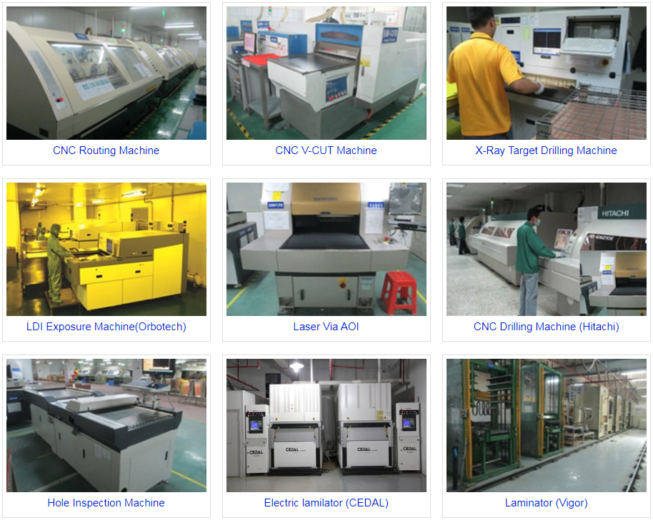
Technology and Equipment: Evaluate the supplier’s manufacturing capabilities, including the equipment and technology they use. Modern equipment and advanced technology can contribute to higher quality and efficiency.
Customization Options: Determine whether the supplier can tailor their services to your project’s unique needs. Flexibility in design, materials, and production quantities is crucial for a successful partnership.
Lead Times and Delivery: Discuss lead times and delivery schedules with potential suppliers. Timely delivery is essential to keeping your project on track.
Pricing and Cost Transparency: Obtain detailed pricing information and ensure transparency in cost breakdowns. Beware of hidden fees that can affect your budget.
Communication and Support: Effective communication and customer support are invaluable. Choose a supplier that is responsive to your inquiries and can provide expert guidance throughout the manufacturing process.
Location and Logistics: Consider the supplier’s location and logistical capabilities, especially if you require international shipping. Efficient logistics can help reduce lead times and costs.
Environmental Responsibility: In today’s environmentally conscious world, inquire about the supplier’s commitment to sustainability and responsible manufacturing practices.
By carefully assessing these criteria and conducting due diligence, you can identify an HDI PCB supplier that aligns with your project’s goals and requirements. Making an informed decision at this stage can lead to a successful and mutually beneficial partnership.
When it comes to selecting a High-Density Interconnect (HDI) PCB supplier, experience and reputation are two crucial factors that demand careful consideration. Let’s delve into why these elements are paramount in your decision-making process.
Experience Matters: An experienced supplier has likely encountered a wide range of challenges and complexities associated with HDI PCB manufacturing. This experience equips them with the knowledge and expertise needed to handle your project efficiently and effectively. They are more likely to offer innovative solutions to design issues, ensuring your PCBs meet the highest quality standards.
Reputation Reflects Reliability: A supplier’s reputation within the industry speaks volumes about their reliability and performance. Positive reviews, testimonials, and references from previous clients are indicators of a supplier’s ability to deliver on their promises. Reputable suppliers are committed to maintaining high-quality standards, which directly benefit your project’s success.
Risk Mitigation: Partnering with an experienced and reputable supplier reduces the risks associated with PCB manufacturing. Their proven track record minimizes the chances of production delays, quality issues, or unforeseen complications that could derail your project timeline and budget.
Innovative Solutions: Seasoned suppliers are often at the forefront of technological advancements in HDI PCB manufacturing. They invest in research and development to stay competitive, offering you access to the latest innovations and design optimizations.
Long-Term Partnerships: Suppliers with a strong reputation and extensive experience are more likely to build long-term partnerships. Such relationships can lead to cost savings, improved communication, and a smoother collaboration on future projects.
In conclusion, when assessing HDI PCB suppliers, prioritize experience and reputation as fundamental criteria. These factors serve as reliable indicators of a supplier’s ability to meet your project requirements, provide expert guidance, and ensure the successful production of high-quality PCBs.
Quality control and adherence to manufacturing standards are pivotal aspects when selecting a High-Density Interconnect (HDI) PCB supplier. Let’s explore why these considerations are vital for ensuring the reliability and performance of your electronic devices.
Consistency in Quality: A reputable HDI PCB supplier maintains stringent quality control measures throughout the manufacturing process. This consistency in quality helps deliver PCBs that meet or exceed your specifications, reducing the likelihood of defects and ensuring reliability in your end products.
Certifications and Standards: Look for suppliers who hold certifications such as ISO 9001, which is a globally recognized standard for quality management systems. These certifications demonstrate a commitment to quality and adherence to established industry standards.
Comprehensive Testing: Inquire about the supplier’s testing procedures. A reliable supplier should conduct a battery of tests, including electrical testing, impedance control, and reliability testing, to identify and rectify any issues before the PCBs are shipped to you.
Material Traceability: Traceability of materials is essential, especially for industries with strict regulatory requirements. Knowing the source and history of materials used in your PCBs can be critical for compliance and troubleshooting.
Failure Analysis: A quality-focused supplier should have a robust system for failure analysis. In the event of defects or issues, they should be able to quickly identify the root cause and implement corrective actions to prevent recurrence.
Continuous Improvement: Choose a supplier that embraces a culture of continuous improvement. Such suppliers are committed to refining their processes and staying updated with the latest industry advancements, ensuring your PCBs benefit from the latest innovations.
Quality Control Documentation: Ensure the supplier provides comprehensive quality control documentation with each shipment. These documents should detail the testing and inspection results, offering transparency and peace of mind regarding the quality of your PCBs.
Customer Feedback Integration: Reputable suppliers actively seek and incorporate customer feedback into their processes. This customer-centric approach helps them address specific project requirements and continuously enhance their service quality.
In summary, quality control and adherence to manufacturing standards are integral components of a reliable HDI PCB supplier. By prioritizing these factors, you can be confident that your chosen supplier is dedicated to delivering PCBs that meet the highest quality and performance expectations.
Selecting the right High-Density Interconnect (HDI) PCB supplier involves more than just evaluating their capabilities—it also requires aligning their offerings with your project’s unique requirements. Here’s how you can tailor your supplier choice to your specific needs:
Customization Options: Discuss your project’s customization requirements with potential suppliers. A supplier capable of accommodating custom designs, materials, and specifications can ensure your PCBs meet your exact needs.
Scalability: Consider your project’s scale and production volume. Choose a supplier that can handle your production needs, whether you require a small prototype run or high-volume production.
Cost Optimization: Evaluate the supplier’s ability to optimize costs while maintaining quality. Cost-efficiency is essential, but not at the expense of performance or reliability.
Lead Times: Assess the supplier’s lead times and delivery schedules. Meeting your project’s timeline is critical, so choose a supplier who can provide realistic delivery commitments.
Technical Support: Inquire about the level of technical support offered by the supplier. A supplier with knowledgeable engineers and support staff can assist in resolving design or manufacturing challenges.
Collaboration and Communication: Effective communication is key to a successful partnership. Choose a supplier that values collaboration and is responsive to your inquiries and feedback.
Logistics and Location: Consider the supplier’s location and logistical capabilities, especially if your project involves international shipping. Efficient logistics can help streamline production and reduce lead times.
Environmental Considerations: If environmental responsibility is a priority for your project, seek suppliers with eco-friendly practices and materials.
By aligning your supplier choice with your project’s specific needs, you can create a partnership that fosters success. A supplier that can adapt to your requirements and provide tailored solutions is more likely to contribute positively to your project’s outcomes.
In conclusion, selecting the best HDI PCB supplier involves careful consideration of experience, reputation, quality control, customization options, and alignment with your project’s unique needs. By systematically evaluating these criteria, you can make an informed decision that ensures the success of your electronic project.
Edge plating for shielding and ground connection
Minimum track width and spacing in mass production around 40μm
Stacked microvias (plated copper or filled with conductive paste)
Cavities, countersunk holes or depth milling
Solder resist in black, blue, green, etc.
Low-halogen material in standard and high Tg range
Low-DK Material for Mobile Devices
All recognised printed circuit board industry surfaces available
HDI PCB Technology Sheet
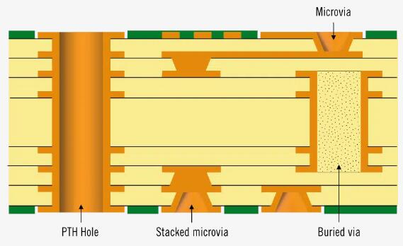
1. 1+N+1 – PCBs contain 1 “build-up” of high-density interconnection layers.
2. i+N+i (i≥2) – PCBs contain 2 or more “build-up” of high density interconnection layers. Microvias on different layers can be staggered or stacked.
3. Copper filled stacked microvia structures are commonly seen in challenging designs.
4. Any Layer HDI – All the layers of a PCB are high density interconnection layers which allows the conductors on any layer of the PCB to be interconnected freely with copper filled stacked microvia structures (“any layer via”). This provides a reliable interconnect solution for highly complex large pin-count devices, such as CPU and GPU chips utilized on handheld and mobile devices.
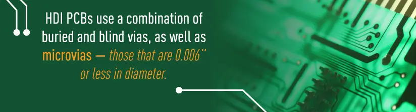
A microvia maintains a laser drilled diameter of typically 0.006″ (150µm), 0.005″ (125µm), or 0.004″ (100µm), which are optically aligned and require a pad diameter typically 0.012″ (300µm), 0.010″ (250µm), or 0.008″ (200µm), allowing additional routing density. Microvias can be via-in-pad, offset, staggered or stacked, non-conductive filled and copper plated over the top or solid copper filled or plated. Microvias add value when routing out of fine pitch BGAs such as 0.8 mm pitch devices and below.
Additionally, microvias add value when routing out of a 0.5 mm pitch device where staggered microvias can be used, however, routing micro-BGAs such as 0.4 mm, 0.3 mm, or 0.25 mm pitch device, requires the use of Stacked MicroVias using an inverted pyramid routing technique.
1. Multilayer copper filled stacked micro via structure
2. 3/3 mil line/space
4/8 mil laser via capture pad size
High temperature FR4
Halogen – Free
Welcome to order HDI PCB from PCBSky at a very competitive HDI PCB price.