PCBSky
service@pcbsky.com +86-755-33583558 Ext 603
Thick / Heavy Copper PCB

How to Choose a Thick/Heavy Copper PCB Supplier?- PCBSky

What is Thick / Heavy Copper PCB

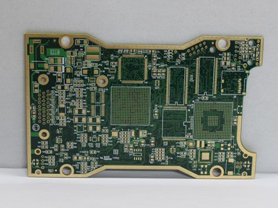
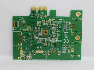
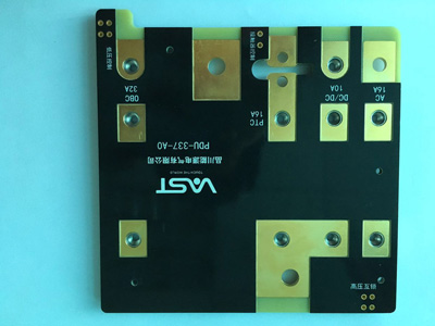
Thick/Heavy copper PCBs (Printed Circuit Boards) are specialized circuit boards designed to handle high current and provide enhanced durability for various electronic applications. They are also known as thick copper PCBs, and they have thicker copper traces or layers compared to standard PCBs. Here are some key points to understand about heavy copper PCBs:

Thick PCB

  1. Thicker Copper Layers: Heavy copper PCBs have copper layers that are significantly thicker than regular PCBs. While standard PCBs typically have copper layers in the range of 1 to 3 ounces per square foot (oz/ft^2), heavy copper PCBs can have copper layers ranging from 4 oz/ft^2 to 20 oz/ft^2 or even more. The increased thickness of copper allows these boards to handle higher current loads without overheating.
  2. High Current Capacity: The primary advantage of heavy copper PCBs is their ability to carry high currents without causing excessive heat buildup. This makes them suitable for power electronics and applications where large amounts of electricity need to flow through the circuit traces without the risk of copper trace damage or melting.
  3. Durability: The thicker copper layers not only enhance current-carrying capacity but also provide better mechanical strength to the PCB. This added durability is essential for applications where the board may experience mechanical stress or environmental factors, such as vibrations, thermal cycling, or exposure to harsh chemicals.
  4. Heat Dissipation: The increased copper thickness helps dissipate heat generated by high-current components more effectively. This can reduce the need for additional heat sinks or cooling mechanisms in the design, making heavy copper PCBs suitable for compact and space-constrained electronic systems.
  5. Cost Considerations: Heavy copper PCBs are more expensive to manufacture than standard PCBs due to the additional copper material and specialized manufacturing processes required. The cost can vary depending on factors such as copper thickness, board size, and the complexity of the design.
  6. Applications: Heavy copper PCBs find applications in various industries, including power electronics, automotive, aerospace, industrial equipment, and renewable energy systems. They are commonly used in power supplies, motor controllers, battery management systems, and any devices or systems that require high current handling.
  7. Design Considerations: Designing heavy copper PCBs requires careful consideration of factors such as trace width, spacing, and thermal management to ensure that the board can effectively handle the expected current loads while maintaining reliability.

In summary, heavy copper PCBs are specialized circuit boards designed to handle high current and provide enhanced durability. They are commonly used in applications where power and reliability are critical, making them a valuable choice in various industries. However, their increased cost and design complexity should be taken into account when selecting them for a particular project.

Design and production difficulties of Thick / Heavy Copper PCB

Heavy Copper PCB

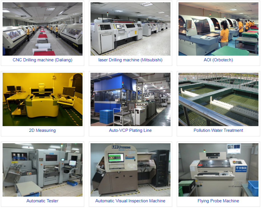
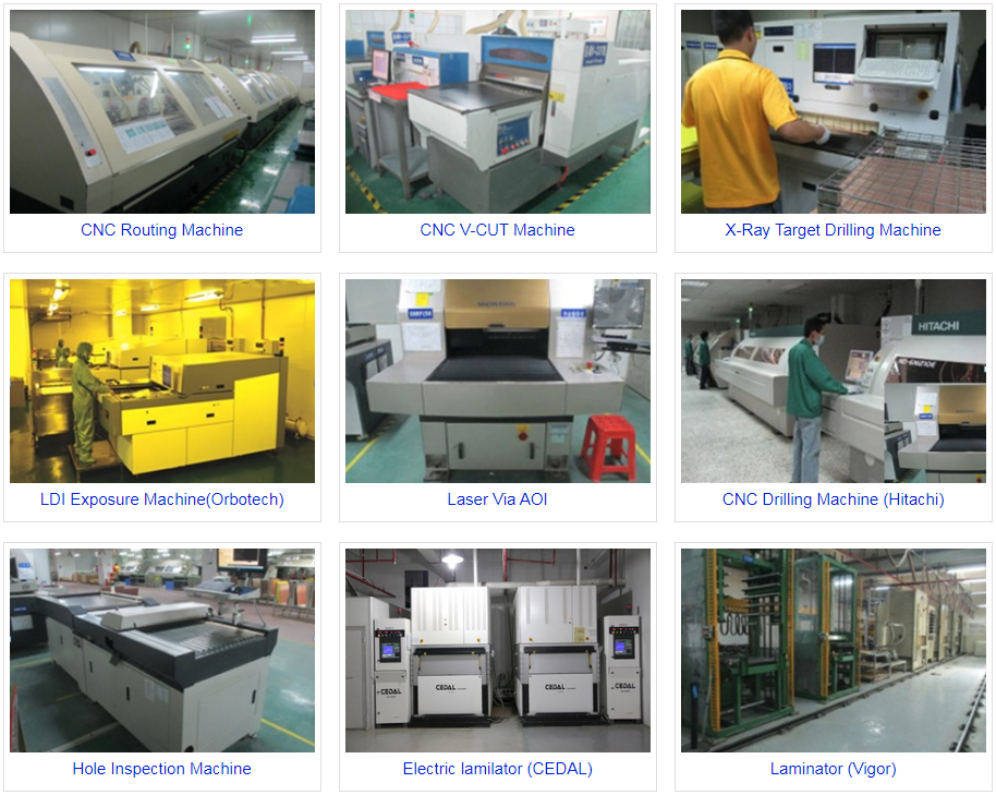
The design and production of heavy copper PCBs come with some additional challenges and complexities compared to regular PCBs. These challenges typically include the following aspects:

  1. Material Selection: Using thicker copper layers requires the selection of appropriate base materials. Common materials like FR-4 may not meet the requirements, so more heat-resistant and high-current-capable materials, such as FR-4 HTG (High Tg), or special ceramic substrates, need to be chosen.
  2. Board Thickness: Heavy copper PCBs often demand thicker substrates, which can add complexity and cost to manufacturing. The thickness of the board affects processes like cutting, drilling, and layer-to-layer connections.
  3. Trace Width and Spacing: Due to the higher currents flowing through heavy copper PCBs, it’s crucial to ensure sufficient trace width and spacing to avoid overheating or electrical issues. This requires precise design and manufacturing.
  4. Thermal Management: The thicker copper layers in heavy copper PCBs can effectively dissipate heat, but optimizing thermal distribution to prevent localized overheating may require the addition of heat sinks, thermal pads, or other thermal management solutions.
  5. Drilling and Plating: Larger hole diameters are needed to accommodate traces within the thick copper layers. This requires more robust drilling equipment and more complex plating processes.
  6. Plating: The electroplating process for heavy copper layers takes more time to ensure an even copper plating. This can increase production time and costs.
  7. Solder Mask: The solder mask for heavy copper PCBs needs to cover more copper to protect the thick copper layers and may require higher soldering temperatures. Special processes and materials may be needed.
  8. Dimensions and Encapsulation: Due to the thicker copper layers, the size of the PCB may increase, potentially limiting its use in certain applications. Additionally, selecting suitable enclosures to accommodate larger components can be a challenge.
  9. Cost: Producing heavy copper PCBs is typically more expensive than regular PCBs due to the additional materials and complex manufacturing processes. This cost factor may limit their use in some projects.

So designing and manufacturing heavy copper PCBs require additional considerations in terms of processes and materials to ensure they meet high-current and durability requirements. These challenges should be taken into account early in the project to successfully produce high-quality heavy copper PCBs.

How to Choose a Thick Copper PCB Supplier

Choosing the right heavy copper PCB supplier is a crucial step in ensuring the success of your project. Here are some considerations to help you select the appropriate heavy copper PCB supplier:

  1. Experience and Reputation: Prefer suppliers with a wealth of experience and a good reputation. Look into the supplier’s track record to see if they have successfully manufactured similar heavy copper PCB projects. Refer to customer reviews and recommendations to gauge their reputation.
  2. Manufacturing Capabilities: Understand the supplier’s manufacturing capabilities, including their production equipment, processes, and technology. Ensure they have advanced equipment and processes suitable for heavy copper PCB manufacturing.
  3. Quality Control: The supplier should have a robust quality control system in place to ensure that each step of production complies with specifications. Check if the supplier holds ISO certifications or other relevant quality certifications.
  4. Engineering Support: Choose a supplier that can provide engineering support to assist you in resolving issues during the design phase and optimizing PCB designs to meet heavy copper requirements.
  5. Cost and Quoting: Consider the supplier’s pricing strategy, but don’t focus solely on price. Make sure you understand their pricing structure and compare it with other suppliers. Note that cheaper options may compromise on quality and support.
  6. Delivery Time: Ensure that the supplier can meet your project’s timeline. Inquire about their production lead times and delivery capabilities to avoid delays.
  7. Samples and Sample Evaluation: Before placing a formal order, request samples from the supplier for evaluation. This helps validate their quality and compliance with your requirements.
  8. Communication and Response Time: The supplier’s response time and communication capabilities are also vital. Ensure that you can easily reach them and receive timely responses.
  9. Location: Consider the supplier’s geographical location as it may impact delivery times and costs. Choosing a supplier closer to your location may reduce transportation costs and delivery times.
  10. Environmental and Social Responsibility: If environmental and social responsibility are important for your project, consider selecting suppliers with clear environmental policies and sustainable practices.

Ultimately, choosing the right heavy copper PCB supplier requires a comprehensive assessment of multiple factors to ensure they can meet your project needs and provide high-quality products and services. Take your time to research and compare different suppliers to make an informed decision.

Our thickest copper PCB can make 12 ounces. However, considering the side eclipse factor, copper thickness of more than 3 ounces should pay special attention to the line width of the inner layer.

Inner 3 oz copper PCB: line width 6/7 mil outer 3 ounces: line width 8/12 mil
Inner layer 4 oz copper PCB: line width line spacing 8/11 mil outer layer 3 ounces: line width line spacing 9/15 mil
Inner 5 oz copper PCB: line width 10/16 mil outer 3 ounces: line width 11/16 mil
Inner 6 oz copper PCB: line width line spacing 12/18 mil outer layer 3 ounces: line width line spacing 14/18 mil

Main Equipments

Leave a Message Email Us

we will contact you within 24 hours.


    • TEL:+86-755-33583558 Ext 603
    • EMAIL:service@pcbsky.com
    • ADDRESS:Add: 407, Kanglan Fortune Center, Fuzhou Avenue, Fuyong Street, Baoan District, Shenzhen, Guangdong 518103, China