
PCB fabrication is the process of manufacturing the bare board. The bare board is then used in the PCB assembly process. We offer both turnkey pcb assembly services and any combination of consigned kits. Turnkey pcb assembly is when we provide the PCB fabrication, components, and assembly labor. Customers can consign components and bare boards as long as the component overages follow our guidelines and the bare board panelization meets our requirements.
Printed circuit board (PCB) assembly is the process of soldering electronic components onto bare boards. Electronic components installed on the bare board can be through-hole and/or surface mount (SMT). If the assembly has both, it is sometimes referred to as a high mix printed circuit board. PCB assembly is one segment of the electronic manufacturing process. Other segments can include cable/wire harness, mechanical/box builds, programming, and functional testing.
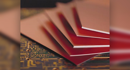
A copper clad laminate is a laminate that has copper foil as its conducting layer. Laminates form the core of a PCB. It consists of layers of metal foil and prepreg (resin + reinforcement material) laminated together with heat and pressure. A laminate used for Printed Circuit Boards can have many different types of metal foil as its conducting layer. These include copper, aluminum, uranium, gold, palladium, carbon fiber, graphite etc. However, copper is used the most due to its excellent electrical characteristics and low cost.
Copper Clad Laminates are classified based on the copper weight, type of resin used, Reinforcement type, glass transition temperature, and various thermal and electrical properties.
The copper foil which is used as the conducting layer of the laminate is available in different specifications as laid out in IPC-4101. This standard also specifies the reinforcement type, the resin system the glass transition temperature range and flammability requirements for making quality copper clad laminate.
Copper Weight: Copper Weight or Copper Thickness in a Printed Circuit Board represents the thickness of 1 ounce of copper rolled out over an area of 1 square foot. It determines the current carrying capacity of a PCB. This is an important parameter that needs to be specified when selecting a copper clad laminate.
Resin: The type of resin used determines the mechanical properties related to stress and strain bearing capacity of the laminate and the thermal characteristics like the rate of expansion and curing properties, which again determine its rate of cross linking among molecular chains which determine its decomposition and glass transition temperature.
| Phenolic | Epoxy | Polyester |
| PTFE | Polyamide/Epoxy | Epoxy/Multi Functional Epoxy |
| Bismaleimide Triazine(BT) | Polyamide | Polyimide Cyanate Ester |
| Cyanate Ester | Epoxy/Phenolic | Flame Resistant |
Reinforcement: The choice of reinforcement used while manufacturing the laminate determines its tooling and drilling characteristics. Cotton and cellulose based laminates do not need to be drilled and can be punched to make a hole in it. Laminates made from a fiber of any kind like, glass, mat glass and quartz require special drilling practices, like closely monitoring the rate of wear of drill bit, the pressure applied to the drill bit and the spindle speed. This is because the thickness and granularity of the glass fibers, the thickness of the copper foil have a huge impact on the number of times a drill bit can be used, which ultimately has an impact on the final cost of making the laminate.
| Cotton Paper | Woven Glass | Mat Glass |
| Cotton Paper/Woven Glass | Woven Glass/Mat Glass | Mat Glass/ Glass Veil |
| Woven Aramid | Woven Quartz Fiber | Woven E-Glass Surface/Cellulose Paper Core |
A copper clad laminate is basically a combination of these layers. The combination determines various mechanical, physical, thermal and electrical properties of the laminate. The properties include the Glass Transition Temperature, the coefficient of thermal expansion. Electrical properties of the board include Dielectric Constant, loss tangent, insulation Resistance, surface resistivity and various other parameters.
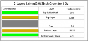
The most common PCB thickness for an FR-4 Printed Circuit Board is 1.57 mm (0.062 inch). This is most the widely used PCB thickness in the industry and is usually the default thickness offered when using the FR-4 substrate.
However, as technology advances and circuits become more complex, the number of layers increases and so does the copper weight. This has resulted in a few more common PCB thickness options that include 93 mils (2.36mm) and 125 mils (3.17mm).
PCB thickness refers to the thickness of the finished Printed Circuit Board. The thickness of the PCB mainly depends on factors such as the number of layers, copper thickness/weight, the substrate used and the operational environment. When discussing the standard PCB thickness, there is no official standard for PCB thickness. But, certain sizes are preferred and have become standard practive among PCB manufacturing companies.
Bar chart
Description automatically generated with medium confidence
Most PCB manufacturers can fabricate a board with a custom thickness, however, this has its drawbacks and challenges. Most of their equipment is already calibrated to a set of certain fixed thickness options. Using a custom thickness can result in them having to adjust their equipment to fit a specific requirement. This can be done but will result in a higher cost and higher turnaround time.
Design factors that impact PCB thickness:
The following design factors need to be considered during the PCB design phase.
Copper thickness: Copper thickness or copper weight plays an important role in deciding the thickness of a PCB. The thicker the copper layer, the more current it can carry. This thickness needs to be decided based on the required application. The standard thickness of the copper layer is 1.4 to 2.8 mils (1 to 2 oz), but the copper thickness can be adjusted if required. As copper thickness increases, the PCB board thickness also increases.
The required copper thickness depends on the application. For example, a copper trance that needs to carry a high power signal will need to be thicker than one that needs to carry a low power signal.
In most cases, the copper thickness is 1 oz so a PCB manufacturing company will try to adjust the thickness of prepreg and core to try and see if they can meet their target PCB thickness.
Board material: The material selection is one of the factors that decide the PCB thickness. Typically, the board fabrication materials include the material for substrate, laminate, solder mask, and silkscreen. Of these, the substrate and laminate material plays important role in deciding the PCB thickness, as these materials form the board’s structure. Usually, the substrate material is epoxy resin, glass weave, or ceramic, and the laminate material is thermoset resin and either paper or cloth layers. These materials not only decide the PCB thickness; they also decide the thermal, mechanical, and electrical properties of the circuit board.
The number of PCB layers: The number of PCB layers is a major factor that decides the PCB thickness. Based on the application requirement, the number of PCB layers can vary. The higher the number of layers, the thicker the board. A standard PCB with thickness of 1.57 mm (0.062 inch) can have 2 to 6 layers. Anything more than this would result in a thicker printed circuit board. The layer count can to up to 60 layers in some cases, so the board thickness can increase significantly.
Size, weight, and flexibility: Selecting the right PCB thickness for your application depends on several factors. A rigid thin PCB board is usually brittle and can break or crack easily. So, this would not be the right board for use in a rugged environment. A thicker rigid board will be more durable. However, in certain cases, flexible boards are required, the thinner the board the more flexible it is. So this is very subjective and depends on the customer’s application.
Manufacturing factors impacted by PCB thickness:
Copper thickness: When a thicker copper layer is used by a PCB the etching process becomes more complicated and can result in the board become more expensive to fabricate.
Depanelization method: The depanelization method is another manufacturing factor that impacts the PCB thickness. Based on the PCB thickness, the fabricator will choose the depanelization method. For example, thicker boards are depanelized by using V-scoring, while the thinner boards are depanelized by using breakaway tabs.
Layer count: When the layer count increases, PCB thickness also increases. The manufacturing of multi-layer boards becomes significantly more challenging.
Factors that need to consider when using a custom PCB thickness:
Usually, PCB manufacturers recommend a set of standard PCB thickness values that they can handle without making any adjustments to their machines. Even though this can be customized, the customer must consider the following points while deciding on a custom PCB thickness:
Know the PCB manufacturer’s equipment capability: It is better to know the PCB manufacturer’s equipment capability; before the PCB design process. It is helpful to avoid the PCB redesign process.
High turnaround time: The customized PCB thickness will need some adjustments to the manufacturing machines. It will increase turnaround time when compared to the standardized PCB thickness.
Additional cost: Yes, some additional costs will need to spend on custom PCB thickness because it may need extra work, material, and manpower than standard thickness PCB.
Turnkey PCB Assembly is the complete PCB Assembly process which includes the fabrication of the board, procurement of components to be placed on the board, the PCB assembly process and other testing or quality control processes that are required to give customers the final assembled printed circuit board.
So, when a customer asks for turnkey PCB assembly, this means that they are looking to get a final PCB board and expect the PCB company to provide all the services required from start to finish.
The alternative to turnkey PCB assembly is to get each step in the PCB assembly process done separately or by different vendors. For example, one vendor would fabricate the board, then someone would be responsible for component procurement, and another company for PCB Assembly and testing of the final board. All this requires a significant amount of coordination.
Interfacial stress is the stress that is generated as a result of soldering two different metals together. Different metals have different CTEs (coefficient of thermal expansion) and thus expand and contract by different amounts as the temperature changes. When two different metals are soldered together, changes in temperature can cause one metal to expand more than the other. Stress caused due to this phenomenon is called Interfacial Stress. An example of this would be joining the leads of a component to a copper pad on a PCB board. The component leads can be a different material from the copper pads. The component leads are soldered onto the copper pads to form an electrical connection. An increase in temperature can cause both metals to expand by different amounts and thus interfacial stress can cause the solder joint to crack and result in a bad connection.
Another area where Interfacial Stress is found in PCBs is within the solder materials itself, due to Intermetallics. Intermetallics are compounds formed when impurities like nickel, gold, palladium and other metals get added into molten solder. These metals are usually present in the leads of surface mount components. In the soldering process, these metals mix with molten solder to form an intermetallic layer (IML). This intermetallic layer is not good because it has a different rate of thermal expansion compared to the layer over and under it. Which can cause interfacial stress failure.
The intermetallic layer of solder joints: a) Infrared heating method,
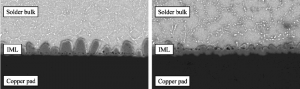
The analysis of stress caused by joining two different metals together is called interfacial stress analysis.
A Peelable solder mask is a type of solder mask that can be peeled off the surface of a printed circuit board. This type of solder mask is used to protect specific areas of a PCB during reflow soldering, wave soldering, or surface finish process. It is applied over the pads or plated through holes prior to the PCB assembly process and prevents the accumulation of excess solder on empty pads during the soldering process. It also protects gold plated contacts which can dissolve in molten solder. Peelable solder mask is easier to remove than regular solder masks.
Peelable solder masks are also used in selective surface finish processes such as soft gold PCB surface finish or Hard gold PCB surface finish. This type of solder mask ensures that the correct finish is only applied to the desired areas of the PCB. The surface finish is a coating on the bare copper area of the PCB to provide a solderable surface and to protect the exposed copper circuitry.
A peelable solder mask is also necessary for the parts that will be manually installed after the automated assembly process.
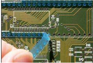
Peelable solder masks are usually applied by screen-printing and are removed after processing at the contracted PCB assembly house. The PCB fabricator can apply the mask in any design or shape on one or several sections per side at a time.
OSP, an abbreviation for Organic Solderability Preservative, it is a method for Printed circuit board Plating. It uses a water based organic compound that selectively bonds to copper and provides an organometallic layer that protects the Copper for Soldering.
What's the difference between "μm" and "oz" for copper weight?
35μm=1oz, 70μm=2oz, and so on
What's the difference between "mm" and "inch" for length?
1mmm=0.039inch, 2mmm=0.078inch, and so on
Sending files email: service@pcbsky.com
Soldermask is the greenish film covering most of the copper area except the pads. If you have access to any electronics devices – you will see that the copper circuit is actually protected by a greenish lacquer like layer – this is the soldermask.
Peelable solder mask is a kind flexible solder mask for area need to be protected during soldering processing,this kind of ink is anti-soldering and could prevent pollution and scratches,it can remain on the protected area of the board until ready for test, and then can easily be peeled away by hand or tools without leaving a residue.
Be sure the preview your gerber files before submitting. Download a gerber viewer(gerber, ViewMate), install, and take a look at your own gerber files. If they don’t look right, or layers do not line up, or if they don’t import at all, stop, fix your output settings and open the gerbers again.
Are there any custom duty and tax for samples and small order?
It depends on the where you are. If you need we can make low invoice value for custom declarations.
For prototype and small quantity order, 2-layer job takes about 7- 8 days lead time, mulitilayer needs about 10-12days lead time. Transportation time can't be controlled by us.
If I order initial small quantity first and order large quantity later on, do I still pay tooling cost?
Tooling cost is one-time charge, it's only applicable to new orders and will be waived when you repeat the order.
We can process Gerber RS-274X, 274D, Eagle, Protel 99se, and DXP formats. But RS-274x gerber format is most welcome, for other file formats, we will re-send gerber files for customer confirmation before processing.
You may contact us at service@pcbsky.com with specifying your quote parameters, if possible attache the PCB file to the email.
Yes. We do not share your designs with anyone and they are only accessible for purchase by you (unless you have published the design). If you are very concerned, we could sign a confidentiality agreements.


