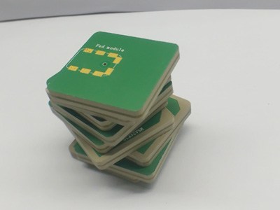
In the rapidly evolving world of communication technology, the backbone of innovation lies in the precision and reliability of printed circuit boards (PCBs). At PCBSky, we take pride in being the trusted experts in communication PCB manufacturing.
The modern world thrives on seamless connectivity, and communication devices are at the heart of this interconnectedness. Whether it’s smartphones, 5G infrastructure, IoT devices, or advanced networking equipment, the performance and efficiency of these technologies heavily rely on the quality of PCBs that power them. This is where we come in.

With years of experience and a deep understanding of the unique demands of the communication industry, we specialize in crafting high-quality, tailor-made PCB solutions that meet the exacting requirements of your communication devices and systems. Our commitment to excellence and innovation has positioned us as a leading player in the field, trusted by companies worldwide to deliver PCBs that enable the world to stay connected.
As your go-to communication PCB manufacturer, we understand the critical role our products play in ensuring seamless communication across the globe. In this age of constant connectivity, you need a partner who can provide the PCB solutions that fuel your innovations. Explore the world of possibilities with us, where precision meets connectivity, and together, we can drive the technology that connects our world.
In modern society, whether in our daily lives or in the business world, communication has become an indispensable part. However, in this highly interconnected world, few people think about the unsung heroes behind communication – Printed Circuit Board (PCB) manufacturing. It is these tiny yet crucial electronic components that connect us with people from all over the world, enabling information to traverse thousands of miles in milliseconds.
PCB manufacturing plays a pivotal role in global communication networks, serving as the essential infrastructure of modern communication. They are considered the indispensable foundation of this field. From your smartphone to internet infrastructure, from satellite communication to medical devices, almost every modern communication tool relies on the precise manufacturing of PCBs.
In this rapidly evolving field, expertise is paramount. Our team consists of experts in communication PCB manufacturing who delve into and comprehend every aspect of this technology. Our experts not only know how to manufacture PCBs, but more importantly, they understand how PCBs become the technological bedrock of seamless connectivity.
We are not just manufacturers; we are drivers of technological innovation. Our team constantly strives to create new solutions, propelling advancements in the field of communication. We are committed to quality assurance, ensuring that each PCB can withstand the test of time and environment, meeting the stringent standards of communication.
PCB manufacturing is not merely a process; it is the backbone of connecting the world, the medium of information transmission, and the bridge for our communication with others. Therefore, we proudly see ourselves as supporters and innovators of modern communication, dedicated to building a more connected and interconnected world. Through outstanding PCB manufacturing, we are collectively forging a future with unimpeded connectivity.
In the realm of communication technology, reliability is non-negotiable. It’s the foundation upon which seamless connections are built, and it’s the essence of what drives our commitment to excellence in PCB manufacturing.
Ensuring reliability in communication technology: Our quality-focused PCB manufacturing.
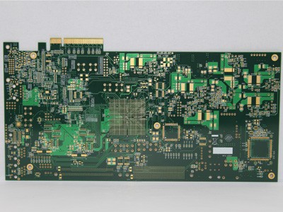
At every step of our PCB manufacturing process, quality is our unwavering focus. We understand that a single glitch can disrupt vital communication channels, which is why we leave no room for compromise. From the selection of premium materials to the precision of our machinery, we take meticulous care to ensure that each PCB meets the highest standards of quality.
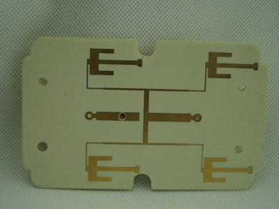
Our quality assurance begins with the design phase, where our expert engineers meticulously craft PCB layouts optimized for reliability and performance. This meticulous attention to detail extends throughout the manufacturing process, encompassing the etching of intricate circuitry, the placement of components with precision, and the application of coatings to safeguard against environmental factors.
The journey from concept to connection: A look at our meticulous manufacturing process.
The path from concept to connection is a journey we undertake with utmost diligence. Our process is a testament to the exacting standards we uphold. It involves stringent testing and inspection protocols at multiple stages, leaving no room for error. We believe in transparency, and we invite you to witness the precision and care that go into every PCB we produce.
Our commitment to reliability also extends to sustainability. We strive to minimize waste and environmental impact throughout the manufacturing process, ensuring that our communication PCBs not only connect people but also protect the planet.
Quality control from start to finish: How we guarantee top-tier PCBs for communication.
From the moment raw materials are selected to the final inspection of finished PCBs, our quality control measures leave nothing to chance. We understand the critical role our PCBs play in enabling global communication networks, and we take that responsibility seriously.
When you choose our PCBs, you’re not just selecting a component; you’re investing in a guarantee of reliability. We stand by our commitment to quality, and it’s our privilege to contribute to the seamless connectivity that defines our modern world.
In a world where communication is paramount, trust in the quality of your PCBs is paramount as well. With our quality-focused approach, we’re not just ensuring reliability in communication technology; we’re elevating it to new heights.
In an era defined by interconnectedness and global communication, the role of printed circuit boards (PCBs) in shaping our world cannot be overstated. These small but powerful electronic components are the unsung heroes behind the seamless connectivity that bridges continents and connects people across the globe. At the heart of this transformative technology are our PCB manufacturing experts, whose impact extends far beyond borders.
A worldwide reach: How our communication PCBs connect the globe.
Our communication PCBs possess a global reach that transcends geographical boundaries. They are the invisible threads that weave together the fabric of modern communication networks. Whether it’s a call made from New York to Tokyo, a data transfer from London to Sydney, or a satellite link connecting remote regions, our PCBs play an essential role in ensuring that these connections remain robust, reliable, and fast.
Partnering with the world’s communication giants: Our experts’ impact.
The influence of our PCB manufacturing experts is not confined to the manufacturing floor. We have forged strategic partnerships with some of the world’s most prominent communication giants, collaborating to advance the very foundations of global communication. Together, we work on innovations that push the boundaries of what’s possible, constantly striving to make communication more efficient, secure, and accessible for all.
Bridging continents through technology: The international presence of our PCBs.
Our PCBs are more than just components; they are enablers of progress. They are present in the communication infrastructure that spans continents, ensuring that information flows seamlessly from one corner of the world to another. Whether it’s supporting telemedicine in remote villages, facilitating emergency services during crises, or powering the backbone of multinational corporations, our PCBs are at the forefront of international connectivity.
In an increasingly interconnected world, where communication transcends borders and time zones, our PCB manufacturing experts are the silent architects of progress. Their expertise and dedication ensure that the globe remains more closely connected than ever before. As we continue to bridge continents through technology, we’re not just manufacturing PCBs; we’re building a world where communication knows no bounds.
In the ever-evolving landscape of communication technology, innovation is not just a goal; it’s a necessity. At the core of our mission lies a forward-looking vision that propels us to shape the future of communication through cutting-edge PCB innovation.
Shaping the future of communication technology through PCB innovation.
Our commitment to innovation is etched into the DNA of our PCB manufacturing process. We believe that the path to tomorrow’s communication excellence begins with pioneering solutions today. Our engineers and researchers continually push the boundaries of what’s achievable, developing PCBs that are not just efficient but transformative.
As the demands of communication technology grow more complex, we remain steadfast in our resolve to provide innovative solutions that enhance connectivity, reduce latency, and elevate the user experience. Whether it’s 5G, Internet of Things (IoT), or the next technological leap, we’re at the forefront, shaping the way we connect tomorrow.
Anticipating trends and demands: Our commitment to forward-thinking manufacturing.
The world of communication technology is marked by rapid change and evolving user needs. We stay ahead of the curve by actively monitoring industry trends and anticipating future demands. Our commitment to forward-thinking manufacturing means that we’re always one step ahead, ready to adapt and innovate to meet the communication needs of the future.
By investing in research and development, fostering a culture of curiosity and creativity, and maintaining close collaborations with industry leaders, we ensure that our PCBs are not just products of today’s demands but are designed to excel in the communication landscape of tomorrow.
Pioneering solutions for evolving communication challenges: Our vision in action.
Our vision is not just a statement; it’s a call to action. It’s a commitment to pioneering solutions for the challenges that lie ahead. From miniaturization and power efficiency to enhanced security and adaptability, we envision PCBs that go beyond conventional expectations.
Our dedicated teams work tirelessly to turn this vision into reality, creating PCBs that not only meet current standards but set new ones. We see every challenge as an opportunity to innovate, every obstacle as a chance to break new ground, and every tomorrow as a canvas upon which we can paint a brighter future for communication technology.
Innovating for tomorrow’s communication needs is not a distant goal; it’s our everyday mission. Through PCB innovation, we’re not just keeping pace with the future; we’re helping to define it.
In the intricate realm of communication technology, one size rarely fits all. That’s why our approach revolves around collaboration and customization, ensuring that your specific communication needs are not just met but exceeded.
Tailoring PCB solutions for your communication needs: Our collaborative approach.
At the heart of our philosophy lies the belief that the best solutions are born through collaboration. We work closely with our clients, engaging in a two-way dialogue to understand the unique challenges and requirements of their communication projects. This collaborative approach allows us to tailor PCB solutions that align perfectly with your needs.
Whether it’s optimizing for size, performance, power efficiency, or any other parameter, our experts are here to listen, adapt, and craft a PCB solution that not only fits but enhances your communication technology.
Partnering with industry leaders: How we co-create communication solutions.
In a fast-paced industry where innovation is key, partnerships matter. We take pride in our collaborations with industry leaders, combining our PCB manufacturing expertise with their insights and experience to co-create cutting-edge communication solutions.
These partnerships bring together the best of both worlds, ensuring that our PCBs are not just technologically advanced but also aligned with industry standards and trends. Together, we push the boundaries of what’s possible, driving innovation that benefits our clients and the broader communication ecosystem.
Your vision, our expertise: Crafting custom communication PCBs together.
Your vision for communication technology is unique, and so should be the PCBs that bring it to life. We offer a dynamic partnership where your ideas and aspirations meet our technical expertise. Whether you have a precise blueprint in mind or need assistance in shaping your vision, we are here to turn your concepts into custom communication PCBs.
Through our collaborative and customized approach, we don’t just provide PCBs; we provide solutions that empower you to achieve your communication goals. Your success is our success, and together, we can forge a path toward communication excellence.
In the world of communication PCB manufacturing, we understand that no two projects are alike. That’s why we embrace collaboration and customization, allowing us to deliver PCB solutions that are as unique as your communication endeavors.
| Application Field | Major Equipment | Related PCB Products | Feature |
| Wi-Fi | Communication base station | Backboard, high-speed multilayer board, high-frequency microwave board, multi-function metal substrate |
Metal based, large size, high multilayer, high frequency materials and mixed pressure |
| Transmission network | OTN transmission equipment, microwave transmission equipment |
Backboard, high-speed multilayer board, high-frequency microwave board |
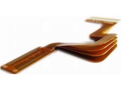
High-speed materials, large size, high multi-layer, high density, multiple back-drilling, rigid-flexible combination, high-frequency materials and mixed pressure |
| data communication | Routers, switches, services/storage devices | Backboard, high speed multilayer board | High-speed materials, large size, high multi-layer, high density, multiple back-drilling, rigid-flexible PCB |
| Fixed network broadband | OLT, ONU and other fiber-to-the-home devices | Backboard, high speed multilayer board | Multi-layer board, rigid-flexible PCB |