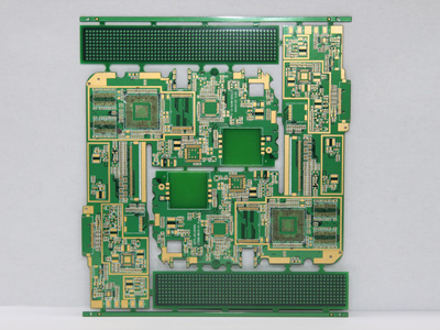
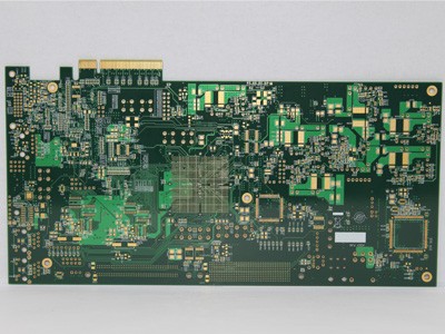
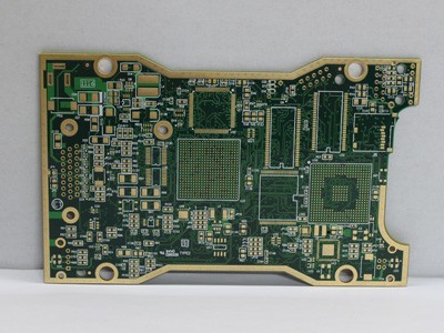
A conventional PCB (Printed Circuit Board) refers to a standard, traditional type of PCB that is commonly used in a wide range of electronic devices and applications. Conventional PCBs serve as the foundation for connecting and interconnecting electronic components to create functional electronic circuits. Here are some key characteristics and features of conventional PCBs:
Layer Structure: Conventional PCBs can have multiple layers, typically consisting of copper traces and insulating layers (usually made of fiberglass-reinforced epoxy resin, known as FR-4). The number of layers can vary based on the complexity of the circuit and design requirements..
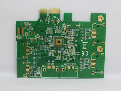
Components and Traces: Electronic components, such as resistors, capacitors, integrated circuits (ICs), and connectors, are mounted onto the PCB's surface. Copper traces are used to connect these components, creating electrical pathways that facilitate the flow of signals and power.
Single-Sided and Double-Sided PCBs: Conventional PCBs can be single-sided (with components and traces on one side) or double-sided (with components and traces on both sides). Single-sided PCBs are simpler and less expensive to manufacture, while double-sided PCBs offer more routing options and higher component density.
Through-Hole Components: Conventional PCBs often incorporate through-hole components, which are inserted into holes drilled through the board. These components are soldered to the PCB to establish electrical connections.
Surface-Mount Components: In addition to through-hole components, surface-mount components (SMD) are commonly used on conventional PCBs. SMD components are soldered directly onto the surface of the PCB, allowing for more compact and lightweight designs.
Traces and Vias: Copper traces are used to connect components and form electrical paths. Vias, which are holes filled with conductive material, enable connections between different layers of the PCB.
Silkscreen and Legend: Conventional PCBs often feature a silkscreen layer, which includes labels, markings, and component outlines to assist with assembly and identification. The legend layer provides additional component markings, such as part numbers and reference designators.
Solder Mask: A solder mask layer is applied to the PCB to cover and protect copper traces and pads while allowing access for soldering during assembly. It is typically green in color but can also be other colors.
Quality Assurance: Quality control measures are implemented during PCB manufacturing to ensure that the board meets design specifications, including dimensions, electrical characteristics, and reliability standards.
Customization: Conventional PCBs are highly customizable to meet specific design requirements. Designers can specify the number of layers, trace widths, hole sizes, and other parameters to tailor the PCB to their application.
Conventional PCBs are used in a wide range of electronic devices, including consumer electronics, industrial equipment, automotive systems, medical devices, and more. They are the foundation of modern electronic circuitry and play a vital role in enabling the functionality of electronic products. Designing and manufacturing conventional PCBs require expertise in PCB design, fabrication, and assembly processes to ensure optimal performance and reliability.
Conventional PCBs can be classified into various categories based on their design, structure, and intended use. Here are some common classifications of conventional PCBs:
Single-Sided PCBs: These PCBs have components and traces on only one side of the board. They are often used for simple and low-cost applications, such as basic electronic circuits and LED displays.
Double-Sided PCBs: Double-sided PCBs have components and traces on both sides of the board. This design provides more routing options and is suitable for moderately complex circuits.
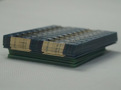
Multilayer PCBs: Multilayer PCBs consist of three or more layers of copper traces separated by insulating material. These PCBs are used in complex electronic devices and can have numerous layers to accommodate high-density components and complex routing.
Rigid PCBs: Rigid PCBs have a solid, inflexible structure and are used in applications where the board will not undergo significant bending or flexing. They are the most common type of PCB.
Flex PCBs (Flexible PCBs): Flex PCBs are designed to be flexible and can bend or conform to the shape of the device they are used in. They are ideal for applications where space is limited or where the PCB needs to fit into a non-planar shape.
Rigid-Flex PCBs (Rigid-Flexible PCBs): Rigid-flex PCBs combine elements of both rigid and flexible PCBs. They have both rigid sections and flexible sections, allowing for a combination of traditional component mounting and flexibility where needed. They are commonly used in devices with complex form factors.
High-Density Interconnect (HDI) PCBs: HDI PCBs are designed to maximize component density and reduce the size of the PCB. They often feature microvias, fine-pitch traces, and advanced manufacturing techniques to achieve high component packing density.
Aluminum PCBs: These PCBs have a base layer made of aluminum, which offers excellent thermal conductivity. They are commonly used in applications where efficient heat dissipation is crucial, such as LED lighting and power electronics.
Copper-Clad PCBs: Copper-clad PCBs have a layer of copper laminated onto a substrate, typically FR-4. They are used in applications where high current-carrying capacity is required.
Lead-Free PCBs: Lead-free PCBs are designed to comply with environmental regulations that restrict the use of lead in electronic products. They use lead-free solder and materials that are RoHS (Restriction of Hazardous Substances) compliant.
High-Frequency PCBs: These PCBs are designed for applications that require the transmission of high-frequency signals, such as RF (Radio Frequency) and microwave applications. They are engineered to minimize signal loss and impedance mismatch.
Specialized PCBs: Some PCBs are designed for specific applications, such as automotive PCBs, medical PCBs, aerospace PCBs, and industrial PCBs. These boards may have unique design considerations and materials to meet the requirements of their respective industries.
The classification of conventional PCBs is based on various factors, including their layer structure, flexibility, materials, and intended use. The choice of PCB type depends on the specific requirements of the electronic device and the design constraints.
 Impedance Control PCB
In today’s electronics industry, Printed Circuit Boards (PCBs) have become a critical component of nearly all electronic devices. For many high-frequency, high-speed, or precision applications such as communication equipment, medical instruments, and military systems, impedance control on the PCB has become paramount. Impedance control involves ensuring that signal transmission on the circuit board stays within…
 Gold Fingers PCB
Gold fingers in PCB fabrication refer to the gold-plated contacts or connectors on the edge of a printed circuit board (PCB). These gold-plated areas are used for various purposes, including providing electrical connections, improving signal quality, and ensuring long-term reliability. Here’s an overview of gold fingers in PCB fabrication: Purpose: Electrical Contact: Gold fingers are…
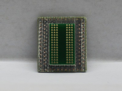 Via in Pad
PCB manufacturing has evolved significantly in recent years, with one of the key advancements being the widespread adoption of Via in Pad (VIP) technology. In modern electronics design and manufacturing, VIP has emerged as a critical factor for enhancing PCB performance and reliability. However, the successful implementation of Via in Pad technology requires rigorous manufacturing…
 High Tg PCB
What is High Tg PCB High Tg PCB stands for “High Glass Transition Temperature Printed Circuit Board.” The glass transition temperature (Tg) is a critical parameter in PCB material selection, and a high Tg PCB is designed to withstand higher temperatures without undergoing a change in its mechanical or electrical properties. Here’s a closer look…
 Edge Plating/Half-hole PCB
When it comes to precision in the world of printed circuit boards (PCBs), there’s a name that stands head and shoulders above the rest: PCBSky, the unrivaled champion of “Unparalleled Precision in Edge Plating /Half-hole PCB Manufacturing.” In today’s fast-paced electronics industry, where every fraction of a millimeter and every fraction of a second count,…
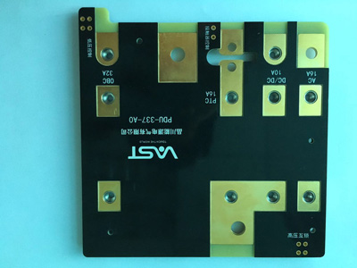 Thick / Heavy Copper PCB
What is Thick / Heavy Copper PCB Thick/Heavy copper PCBs (Printed Circuit Boards) are specialized circuit boards designed to handle high current and provide enhanced durability for various electronic applications. They are also known as thick copper PCBs, and they have thicker copper traces or layers compared to standard PCBs. Here are some key points…
 Hard Gold PCB
What is a hard gold PCB? A “Hard Gold PCB” refers to a type of printed circuit board (PCB) that has gold plating on its surface. Gold plating is used in PCB manufacturing for various reasons, including its excellent conductivity, corrosion resistance, and aesthetic appeal. Here’s some information about hard gold PCBs: Gold Plating Types:…
Conventional PCBs (Printed Circuit Boards) find a wide range of applications across almost all electronic devices and fields. Here are some common applications of conventional PCBs:
Consumer Electronics: Conventional PCBs are extensively used in various consumer electronic products, including smartphones, tablets, televisions, audio systems, gaming consoles, digital cameras, and more. They are employed for connecting and supporting a variety of electronic components, from microprocessors to displays and audio devices.
Industrial Automation: The field of industrial automation uses conventional PCBs to control and monitor production lines, robots, sensors, PLCs (Programmable Logic Controllers), and various industrial equipment. These PCBs have requirements for stability and reliability.
Medical Devices: Medical equipment such as medical imaging devices, heart monitors, blood glucose meters, and drug delivery systems rely on conventional PCBs to support their electronic control and data processing functions.
Automotive and Transportation: Conventional PCBs are widely employed in the automotive industry for engine control units, dashboards, navigation systems, safety systems, in-car entertainment systems, and autonomous driving technologies, among others.
Communication Equipment: Conventional PCBs are used in the manufacturing of communication equipment, including base stations, routers, switches, fiber optic communication devices, and satellite communication equipment. High-frequency PCBs are especially important in these applications.
Military and Defense: The military and defense sector requires highly reliable PCBs to support critical tasks such as radar systems, missile control, communication devices, and flight control systems.
Aerospace: In the aerospace field, conventional PCBs are used in flight control, navigation, communication, and instrumentation systems to ensure the safety and performance of aircraft.
Energy: The energy industry uses conventional PCBs to monitor and control power distribution, grid equipment, renewable energy systems, and oil and gas exploration equipment.
Electronic Testing and Measurement: Conventional PCBs are manufactured for electronic testing, measurement, and instrumentation devices, including oscilloscopes, multimeters, and signal generators.
Home Electronics: Conventional PCBs support home electronic products such as smart home systems, home security systems, smart TVs, and home office equipment.
In summary, conventional PCBs are integral components in modern electronic devices and are present in almost every field, ranging from consumer electronics in everyday life to industrial, medical, military, aerospace, and high-specialization applications. Their significance lies in providing a reliable means to connect, support, and control electronic components, enabling various devices and technologies to function properly.
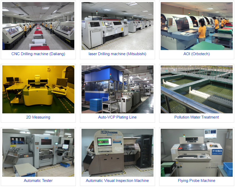
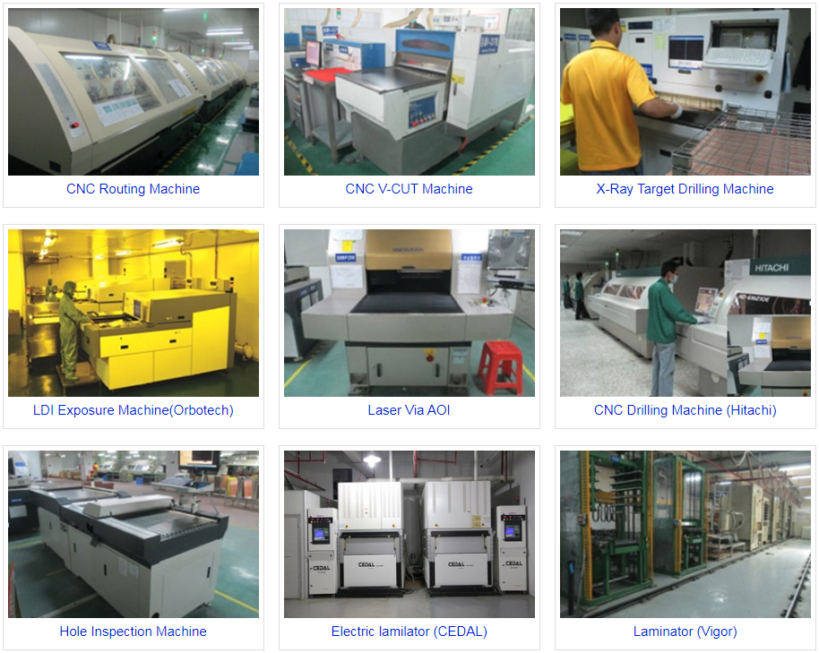
Choosing a suitable conventional PCB (Printed Circuit Board) supplier is crucial to the success of your electronic product. Here are some steps and considerations to help you select the right supplier:
Define Your Requirements:
Clearly outline your project requirements, including the number of layers, board size, material specifications, and any specific design constraints or technology requirements.
Supplier Experience:
Look for PCB suppliers with a proven track record and extensive experience in manufacturing conventional PCBs. Experience is vital as it often correlates with expertise and reliability.
Certifications and Standards:
Ensure that the supplier adheres to industry standards and certifications, such as ISO 9001, ISO 14001, IPC (Association Connecting Electronics Industries) standards, and RoHS compliance. These certifications demonstrate a commitment to quality and environmental responsibility.
Technical Capabilities:
Assess the supplier's technical capabilities, including their equipment, manufacturing processes, and design support services. Verify that they have the technology and expertise to meet your project's specific requirements.
Quality Control:
Inquire about the supplier's quality control procedures. Ask about their inspection and testing processes to ensure the PCBs meet your quality standards. They should conduct electrical testing and may offer additional testing options.
Prototyping and Sampling:
Request samples or prototypes to evaluate the supplier's manufacturing quality and capabilities. This allows you to assess the quality of their PCB fabrication and assembly.
Lead Times and Production Capacity:
Understand the supplier's lead times and production capacity. Ensure they can meet your project deadlines and handle the required production volumes.
Cost and Pricing Structure:
Compare the pricing structure of multiple suppliers. Be cautious of significantly lower prices, as they may indicate compromised quality. Request detailed quotations that include all costs, such as setup fees, tooling charges, and shipping.
Communication and Support:
Evaluate the supplier's communication skills and responsiveness. A good supplier should be accessible and willing to provide ongoing support throughout the manufacturing process.
Location and Logistics:
Consider the supplier's location and logistics. Proximity can reduce shipping costs and lead times. Ensure they have reliable shipping and handling procedures.
References and Reviews:
Ask for references or check online reviews and testimonials from other customers who have worked with the supplier. This can provide valuable insights into their performance and reliability.
Environmental Responsibility:
If environmental responsibility is important to your organization, inquire about the supplier's environmental practices and certifications, such as ISO 14001.
Confidentiality and Security:
If your project involves sensitive or proprietary information, discuss confidentiality and security measures with the supplier to ensure the protection of your intellectual property.
Long-Term Partnership:
Consider the potential for a long-term partnership. Building a strong relationship with a reliable supplier can lead to smoother collaboration on future projects.
By carefully evaluating these factors and conducting due diligence, you can identify a conventional PCB supplier that aligns with your project's requirements, quality standards, and long-term goals. Effective communication and ongoing collaboration with your chosen supplier are key to a successful partnership.
| Feature | Capability |
| Quality Grade | Standard IPC 2 |
| Number of Layers | 1 - 32layers |
| Order Quantity | 1pcs - 10,000,000 pcs |
| Build Time | 2days - 5weeks (Expedited Service) |
| Material | FR-4 Standard Tg 150°C, FR4-High Tg 170°C, FR4-High-Tg 180°C FR4-Halogen-free, FR4-Halogen-free & High-Tg |
| Board Size | Min 6*6mm | Max 600*700mm |
| Board size tolerance | ±0.1mm - ±0.3mm |
| Board Thickness | 0.4mm - 3.2mm |
| Board Thickness Tolerance | ±0.1mm - ±10% |
| Copper Weight | 0.5oz - 6.0oz |
| Inner Layer Copper Weight | 0.5oz - 2.0oz |
| Copper Thickness Tolerance | +0μm +20μm |
| Min Tracing/Spacing 3mil/3mil | 3mil/3mil |
| Solder Mask Sides | As per the file |
| Solder Mask Color | Green, White, Blue, Black, Red, Yellow |
| Silkscreen Sides | As per the file |
| Silkscreen Color | White, Blue, Black, Red, Yellow |
| Surface Finish | HASL - Hot Air Solder Leveling |
| Lead Free HASL | RoHS |
| ENIG - Electroless Nickle/Immersion Gold | RoHS |
| ENEPIG - Electroless Nickel Electroless Palladium Immersion Gold | RoHS |
| Immersion Silver | RoHS |
| Immersion Tin | RoHS |
| OSP -Organic Solderability Preservatives | RoHS |
| Min Annular Ring | 3mil |
| Min Drilling Hole Diameter | 6mil, 4mil-laser drill |
| Min Width of Cutout (NPTH) | 0.8mm |
| NPTH Hole Size Tolerance | ±.002" (±0.05mm) |
| Min Width of Slot Hole (PTH) | 0.6mm |
| PTH Hole Size Tolerance | ±.003" (±0.08mm) - ±.006" (±0.15mm) |
| Surface/Hole Plating Thickness | 20μm - 30μm |
| SM Tolerance (LPI) . | 003" (0.075mm) |
| Aspect Ratio | 1.10 (hole size: board thickness) |
| Test 10V - 250V, flying probe or testing fixture | |
| Impedance tolerance | ±5% - ±10% |
| SMD Pitch | 0.2mm(8mil) |
| BGA Pitch | 0.2mm(8mil) |
| Chamfer of Gold Fingers | 20, 30, 45, 60 |
| Other Techniques | Gold fingers, Blind and Buried Holes, peelable solder mask, Edge plating, Carbon Mask, Kapton tape, Countersink/counterbore hole, Half-cut/Castellated hole, Press fit hole, Via tented/covered with resin, Via plugged/filled with resin, Via in pad, Electrical Test |