When you require customized circuit board design and layout solutions, our team is ready to provide outstanding service tailored to meet your unique needs. As experts in the field of circuit board design and layout, we understand the uniqueness of each project, and we are committed to delivering personalized and innovative solutions for you.
In modern electronics manufacturing, the design and layout of circuit boards play a crucial role. A well-crafted circuit board can not only enhance performance and reliability but also save costs and reduce manufacturing lead times. Therefore, choosing a trusted partner to meet your circuit board design needs is paramount.
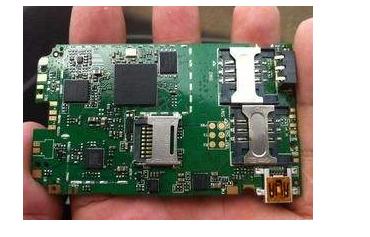
Our professional team boasts years of experience and expertise in various types of circuit board layouts, including single-layer, double-layer, and multi-layer circuit boards. Regardless of the scale of your project or whether you require prototype designs or mass production, we are capable of delivering high-quality and efficient services.
Our goal is to ensure that your circuit board design and layout align with your technical requirements, cost budget, and schedule. By partnering with us, you can rest assured that your project will be handled by an experienced and professional team to achieve optimal performance and reliability.
Whatever your project’s requirements for PCB design and layout solutions, we will go the extra mile to meet your needs. Please get in touch with us, and let’s embark on creating exceptional circuit board designs and layouts for your project.
When it comes to customized circuit board design and layout solutions, our team is dedicated to providing exceptional services tailored to your unique requirements. As experts in the field of circuit board design and layout, we deeply understand the distinctiveness of each project and are committed to delivering personalized, innovative solutions that precisely meet your needs.
Customized Solutions:
Within our team, we specialize in comprehending the specific demands of your project. Recognizing that each project is distinctive, we employ a customized approach to ensure that our solutions align perfectly with your expectations. No matter what your project requires in terms of circuit board design and layout solutions, we are here to provide a personalized service tailored to your specifications.
Experienced Professional Team:
Our professional team brings years of hands-on experience in circuit board design and layout. Regardless of the scale of your project, we can offer expert support. We are proficient in various types of circuit board layouts, including single-layer, double-layer, and multi-layer boards. This means that whether you need prototype designs or mass production, we have the relevant expertise and skills to bring your vision to life.
Performance and Reliability:
In today’s world of electronics, achieving top-notch performance and reliability is paramount. By optimizing circuit board design, we help you enhance product performance to meet the rigorous demands of high-end applications. Simultaneously, our designs are crafted with a primary focus on reliability, ensuring that your circuit boards perform exceptionally well over extended periods. We do not just prioritize innovative design but also practical working performance.
Cost-Effectiveness:
We recognize that cost-effectiveness plays a pivotal role in the success of your projects. Our design methods are crafted to minimize manufacturing costs without compromising on quality standards. Through our efficient design and layout approaches, you can also significantly reduce production lead times, allowing you to introduce your products to the market faster and more competitively.
Professional Consultation and Support:
Our commitment to excellence extends to offering expert project consultation. We ensure that your circuit board design and layout not only meet but exceed your expectations. We work closely with you throughout the project to gain a deep understanding of your requirements, enabling us to provide the best possible solutions. Furthermore, our support doesn’t end with design; we offer continuous assistance throughout the project’s lifecycle to ensure seamless progress.
High-Quality Assurance:
Quality is the cornerstone of our work. We implement rigorous quality control processes to ensure that every circuit board design meets and even surpasses high standards. Our comprehensive testing and verification procedures are in place to validate circuit board performance and reliability. With us, you can rest assured that your project will be supervised with an unwavering focus on top-notch quality.
Suitable for Various Project Scales:
Whether your project entails prototype designs or large-scale mass production, we have the versatility to cater to your needs. We understand that different projects may come with varying scales and requirements, and we offer flexible support to ensure the successful completion of your project, no matter the size.
Partnership:
We aren’t just your circuit board design and layout service provider; we are your dedicated partners. We are committed to forging long-term partnerships, growing together, and adapting to your evolving needs. Think of us as your circuit board experts, providing comprehensive support for all your projects, big or small.
Within our team, we invest not only expertise but also passion into every project. Whatever your circuit board design and layout requirements may be, we strive to meet and exceed your expectations with innovation, quality, and exceptional service. Get in touch with us today, and let’s collaborate to create outstanding circuit board design and layout solutions that elevate your project to new heights.
5.High difficulty design experience
We are good at high frequency and high speed, high density, digital analog mixing, high power, high current, RF, ate, software and hardware board, high speed backplane, etc.; we have 2000 + PCB layout experience every year.
6.Abundant technical resources
Chip companies cooperate in the early stage, accumulate forward-looking technology, synchronize cutting-edge technologies, master the most advanced technical information, and fully consider EMI, EMC and manufacturability design.
7.High quality management system
Standardized design management system, strict inspection, layer by layer check, do not let go of any mistakes and details, to ensure that the failure rate is zero, 1000 + customers credit accumulation.
8.High standards of confidentiality
High standard security measures, signing confidentiality agreement, the company’s designer computer encryption, all documents need to be approved for export, to ensure that the documents are 100% confidential.
9.Ability to design
The maximum number of layers is 42
The minimum trace width is 2.4mil
Maximum pin number 110000 +
Maximum connection number 78000+
The minimum distance between BGA pins is 0.3mm
The maximum number of bga-pins is 2912
The highest speed signal is 60GHz
The minimum trace spacing is 2.4mil
10.The Design cycle
| Pin number of single board | Design delivery date (working days) |
| Within 1000 | 3-5days |
| 2000-3000 | 5-7days |
| 4000-5000 | 8-12days |
| 6000-7000 | 12-15days |
| 8000-9000 | 15-18days |
| 10000-13000 | 18-20days |
| 14000-15000 | 20-22days |
| 16000-20000 | 22-30days |
11.The Design flow
Customer needs to provide information
Schematic diagram (schdoc, DSN or SCH) or netlist, structure diagram (DXF), package library (datasheet manual for newly built packages), design requirements, etc.
Layout and wiring review
According to the design specification, design instruction, customer design requirements and related checklist. After the start of the project, our engineers will check the schematic DRC, check the structure and other electrical design requirements. If there is any question, we will report it to the customer immediately.
Customer layout confirmation
Provide layout files and structure files for customers to review layout; customers confirm layout rationality, stacking scheme, impedance scheme, structure, packaging, and confirm wiring parameters.
Design data output
PCB source file, Gerber file, assembly file, steel mesh file, structure file, etc. After the PCB layout design is completed, our engineers conduct mutual inspection, including DFM inspection, QA inspection, EMC inspection. After the customer confirms that it is OK, Gerber and other production files will be issued.