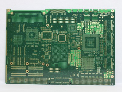
A "blind and buried PCB" is a type of printed circuit board (PCB) that combines the features of both blind vias and buried vias. Blind and buried vias are specialized interconnection techniques used to create complex PCBs with multiple layers and various connections. Here's what you need to know about blind and buried PCBs:
Blind Vias: Blind vias are vias that connect one or more inner layers of a PCB to the outer layers but do not penetrate through the entire board. They are "blind" because they only go partway through the board. These vias are typically used to make connections between the outer layers and one or more specific inner layers of the PCB.
Buried Vias: Buried vias, on the other hand, are vias that connect one or more inner layers of the PCB but do not extend to the outer layers. They are "buried" within the PCB stackup. These vias are used for creating connections between inner layers while keeping them hidden from the outer layers.
Blind and Buried Vias: A blind and buried PCB combines these two techniques. It has vias that are both blind and buried, meaning they connect specific inner layers to one or both outer layers and are hidden within the PCB stackup. This allows for complex multilayer PCB designs with a high degree of customization.
Key advantages of blind and buried PCBs:
Enhanced Signal Integrity: By using blind and buried vias, you can route high-speed signals through inner layers, reducing signal interference and improving signal integrity.
Higher Component Density: These PCBs provide greater flexibility in component placement and routing, leading to higher component density and more compact designs.
Reduced EMI: The hidden vias help reduce electromagnetic interference (EMI), which is crucial in sensitive electronic applications.
Security and Reliability: Critical components and traces can be buried within the PCB, offering improved security and reliability in applications where tampering or environmental factors are concerns.
Customization: Blind and buried PCBs are often used in custom designs where specific layer configurations and routing are required.
It's important to note that designing and manufacturing blind and buried PCBs is more complex and costly than standard PCBs or those with just blind or buried vias. The additional complexity arises from the precise drilling, plating, and layer stacking processes involved. Therefore, they are typically used in applications where the benefits of enhanced signal integrity, compact design, and reduced EMI outweigh the added manufacturing complexity and cost.
Manufacturing blind and buried PCBs can be more challenging and complex compared to standard double-sided or multilayer PCBs. The difficulties in manufacturing these specialized PCBs arise from several factors:
Precise Drilling: Blind and buried vias require precise drilling to connect specific layers while not penetrating through the entire board. Achieving this precision can be difficult and may necessitate advanced drilling techniques and equipment.
Layer Alignment: Ensuring accurate alignment of the PCB layers during the manufacturing process is critical. Misalignment can result in vias not connecting where they should or causing short circuits.
Increased Complexity: The complexity of the layer stackup is significantly higher in blind and buried PCBs. Managing multiple layers and their connections adds complexity to the manufacturing process.
Additional Processing Steps: Blind and buried vias require additional processing steps, such as laser drilling, plating, and filling with conductive material. Each of these steps must be performed with precision to maintain the integrity of the PCB.
Increased Cost: The additional processing steps, specialized equipment, and labor required for blind and buried PCBs contribute to higher manufacturing costs compared to standard PCBs.
Testing Challenges: Verifying the integrity and functionality of blind and buried vias can be challenging. Specialized testing methods may be needed to ensure that all connections are working correctly.
Materials and Substrates: The choice of materials and substrates is critical in blind and buried PCBs. The materials used must meet specific electrical and thermal requirements while also being compatible with the manufacturing process.
Limited Design Flexibility: Blind and buried PCBs are less forgiving when it comes to design errors. Any mistakes in the design, such as incorrect via placements or insufficient clearance, can be difficult to rectify during manufacturing.
Expertise and Experience: Manufacturing blind and buried PCBs requires specialized knowledge and experience. Not all PCB manufacturers are equipped to handle these complex boards, which may limit your choice of manufacturing partners.
Lead Times: Due to the increased complexity and additional processing steps, lead times for blind and buried PCBs can be longer compared to standard PCBs. This can impact project schedules.
Despite these challenges, blind and buried PCBs offer significant benefits in terms of signal integrity, component density, and reduced electromagnetic interference in certain applications. Designers and manufacturers must carefully weigh the advantages against the difficulties and costs when deciding to use blind and buried vias in their PCBs.
 HDI PCB
Choosing the best High-Density Interconnect (HDI) PCB supplier is crucial for the performance of electronic products. In a highly competitive market, the quality of circuit boards directly impacts product reliability and performance. This article will guide you on making informed supplier choices. HDI PCBs have become a vital component of modern electronic devices, enabling smaller,…
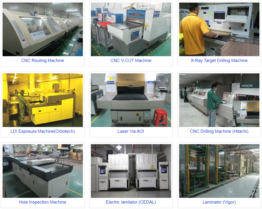
Ensuring the quality of blind and buried PCBs is crucial, given the complexity and specialized manufacturing processes involved. Quality assurance measures are essential to guarantee that the finished PCBs meet the required standards and specifications. Here are some key steps and considerations for quality assurance of blind and buried PCBs:
Design Review:
Begin with a thorough review of the PCB design. Check for any design errors or issues that could affect the integrity of the blind and buried vias, such as incorrect via placements, insufficient clearance, or layer misalignments.
Material Selection:
Ensure that the materials used in the PCB stackup are of the appropriate quality and meet the required electrical and thermal specifications. Verify that they are compatible with the manufacturing processes, including laser drilling and plating.
Manufacturing Process Control:
Work closely with the PCB manufacturer to establish and monitor strict process controls. This includes ensuring precision in drilling, plating, and filling of the blind and buried vias.
Regularly inspect and calibrate the manufacturing equipment to maintain consistency and accuracy.
Testing and Inspection:
Implement comprehensive testing and inspection procedures to verify the quality of the finished PCBs.
Use advanced techniques such as X-ray inspection to ensure the integrity of the blind and buried vias, as they are not visible from the surface.
Conduct electrical testing to confirm that all connections are functioning correctly.
Perform visual inspections to check for any physical defects or anomalies.
uality Control Documentation:
Maintain detailed records and documentation throughout the manufacturing process. This includes documenting design specifications, process parameters, inspection results, and any deviations from the expected standards.
Establish a traceability system to track each PCB's history and manufacturing steps.
Reliability Testing:
Subject a sample of the blind and buried PCBs to reliability testing to ensure they can withstand environmental factors, thermal stress, and other conditions relevant to the intended application.
Quality Assurance Team:
Assemble a dedicated quality assurance team or assign responsible individuals within your organization to oversee the entire process from design to production.
Conduct regular internal audits to identify and address potential issues.
Supplier Quality Management:
If working with an external PCB manufacturer, establish strong supplier quality management practices. Conduct regular audits of the manufacturing facility to ensure compliance with quality standards.
edback and Continuous Improvement:
Encourage open communication between your design team and the manufacturer. Address any issues or concerns promptly to prevent recurring problems.
Continuously seek opportunities for process improvement and cost optimization.
Compliance with Industry Standards:
Ensure that the blind and buried PCBs adhere to industry-specific standards and regulations relevant to your application, such as IPC (Association Connecting Electronics Industries) standards.
Quality assurance of blind and buried PCBs requires diligence, collaboration, and a commitment to excellence throughout the design and manufacturing process. By implementing these measures, you can minimize the risk of defects and ensure that the final product meets the highest quality standards.
PCBSky specializes in producing various blind buried multilayer PCBs, including HDI PCBs and blind buried hybrid circuit boards.