Are you looking for the perfect manufacturer for your rigid flex PCBs? Look no further! In this article, we will unlock the secrets to finding the ideal manufacturer that will meet all your needs.
Rigid flex PCBs offer a unique solution for electronic devices, combining the flexibility of a flexible PCB with the durability of a rigid PCB. However, finding the right manufacturer can be a daunting task. That’s why we’re here to guide you through the process and help you make an informed decision.
With our expert tips and insights, you’ll discover the key factors to consider when choosing a manufacturer for your rigid flex PCBs. From quality and reliability to cost-effectiveness and customer support, we’ll cover it all.
Don’t settle for less when it comes to your rigid flex PCBs. Find the perfect manufacturer and unlock the potential of your electronic devices. Let’s get started on this exciting journey together!
Rigid flex PCBs offer a unique solution for electronic devices, combining the flexibility of a flexible PCB with the durability of a rigid PCB. This innovative design allows for greater design flexibility, reduced space requirements, and improved reliability. With rigid flex PCBs, electronic devices can be made smaller, lighter, and more resistant to shock and vibration.
One of the key benefits of rigid flex PCBs is their ability to withstand harsh environments. The combination of rigid and flexible materials ensures that the PCB can withstand extreme temperatures, moisture, and even exposure to chemicals. This makes them ideal for applications in industries such as aerospace, automotive, medical, and military, where reliability is of utmost importance.
Another advantage of using rigid flex PCBs is their cost-effectiveness. While the initial manufacturing costs may be slightly higher compared to traditional PCBs, the overall cost savings can be significant. The reduced need for connectors, cables, and additional components can result in lower assembly costs and improved product reliability.
Rigid flex PCBs find applications in a wide range of industries and products. Their unique design allows for the creation of complex electronic devices that would otherwise be challenging to achieve with traditional PCBs. Here are some common applications of rigid flex PCBs:
1. Wearable devices: The flexibility of rigid flex PCBs makes them ideal for wearable technology such as smartwatches, fitness trackers, and medical devices. The ability to bend and conform to the shape of the body ensures a comfortable fit and optimal performance.
2. Aerospace and defense: Rigid flex PCBs are widely used in the aerospace and defense industries due to their ability to withstand extreme conditions and vibrations. They are used in avionics systems, missile guidance systems, and radar systems, among others.
3. Medical devices: Rigid flex PCBs are used in various medical devices, including pacemakers, hearing aids, and diagnostic equipment. Their compact size and reliability make them essential for critical medical applications.
4. Automotive: Rigid flex PCBs are used in automotive applications such as infotainment systems, GPS navigation systems, and advanced driver-assistance systems (ADAS). Their ability to withstand high temperatures and vibrations makes them suitable for the demanding automotive environment.
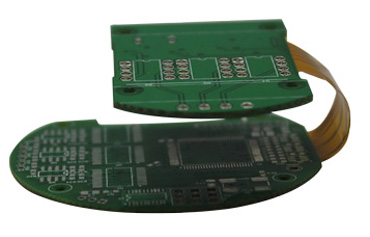
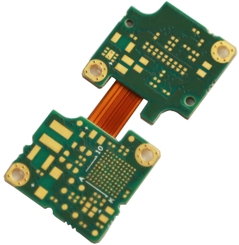
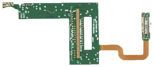
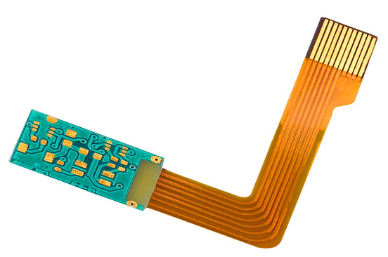
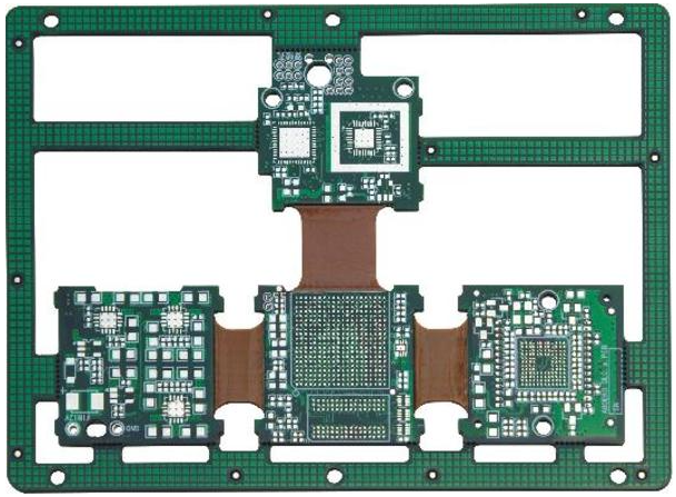
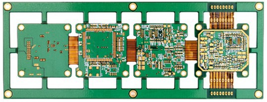
Rigid Flex PCBs are hybrid circuit boards that integrate both rigid and flexible substrates into a single unit. They consist of rigid sections that provide stability and support for components and flexible sections that enable bending and folding. The combination of these two types of materials creates a robust and versatile PCB solution.
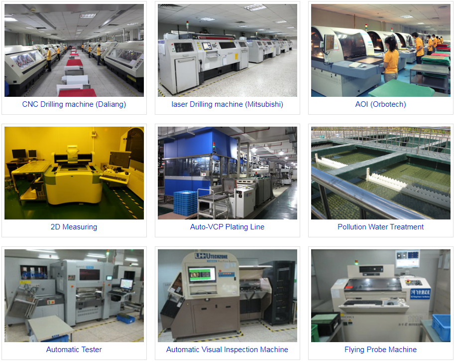
The manufacturing process of rigid flex PCBs is complex and requires specialized equipment and expertise. Understanding this process is crucial when evaluating potential manufacturers. Let’s take a closer look at the key steps involved:
1. Design and layout: The first step in manufacturing rigid flex PCBs is designing the circuit layout. This involves determining the size, shape, and arrangement of the rigid and flexible sections. Design software is used to create a digital representation of the PCB, which is then used to generate the manufacturing files.
2. Material selection: Choosing the right materials is essential for the performance and reliability of the rigid flex PCB. The materials should be able to withstand the intended operating conditions, including temperature variations, moisture, and chemical exposure. Common materials used in rigid flex PCBs include polyimide, FR-4, and copper foils.
3. Manufacturing and assembly: The manufacturing process involves several steps, including drilling, plating, and laminating. Holes are drilled into the rigid and flexible sections of the PCB, and then the layers are plated with copper. The layers are then laminated together using heat and pressure. After lamination, the PCB is routed and the components are assembled using surface mount technology (SMT) or through-hole technology (THT).
4. Testing and inspection: Once the PCBs are assembled, they undergo rigorous testing and inspection to ensure they meet the required quality standards. This includes electrical testing, thermal testing, and visual inspection. Any defects or issues are identified and corrected before the PCBs are shipped to the customer.
When it comes to choosing a manufacturer for your rigid flex PCBs, there are several factors that you need to consider. These factors will help you evaluate the capabilities and reliability of potential manufacturers, ensuring that you make an informed decision. Here are some key factors to keep in mind:
1. Experience and expertise: Look for a manufacturer with extensive experience in designing and manufacturing rigid flex PCBs. They should have a deep understanding of the unique challenges and requirements of this technology. A manufacturer with a proven track record and a team of skilled engineers will be better equipped to meet your specific needs.
2. Quality and reliability: Quality is of utmost importance when it comes to rigid flex PCBs. Look for a manufacturer that has a robust quality control process in place. They should adhere to international quality standards and have certifications such as ISO 9001. Additionally, ask for customer references and testimonials to gauge the manufacturer’s reputation for delivering high-quality products.
3. Manufacturing capabilities: Assess the manufacturer’s manufacturing capabilities to ensure they can handle your project requirements. Consider factors such as their production capacity, equipment and technology, and ability to handle complex designs. A manufacturer with advanced equipment and a well-equipped facility will be better positioned to meet your production needs.
4. Cost-effectiveness: While cost should not be the sole determining factor, it is important to consider the pricing structure of potential manufacturers. Request quotes from multiple manufacturers and compare them based on the services offered, quality, lead times, and overall value for money. Keep in mind that the cheapest option may not always be the best in terms of quality and reliability.
5. Customer support: Evaluate the manufacturer’s level of customer support and responsiveness. Communication is key throughout the manufacturing process, and you need a manufacturer that is proactive and responsive to your needs. Consider factors such as their ability to provide timely updates, address any issues or concerns, and offer technical support when needed.
Once you have a list of potential manufacturers, it’s time to dive deeper and evaluate their capabilities and suitability for your project. Here are some steps you can take to research and evaluate potential manufacturers:
1. Online research: Start by researching potential manufacturers online. Visit their websites, read their company profiles, and learn more about their capabilities and services. Look for case studies, testimonials, and customer reviews to get an idea of their track record and customer satisfaction.
2. Reach out for information: Contact the manufacturers directly and request more information about their capabilities, certifications, and past projects. Ask for samples or prototypes to assess the quality of their work. This will give you a better understanding of their capabilities and help you determine if they are a good fit for your project.
3. Visit the facility: If possible, arrange a visit to the manufacturer’s facility. This will allow you to see their manufacturing processes firsthand and assess the quality of their equipment and infrastructure. Meeting the team in person can also help you gauge their level of expertise and professionalism.
4. Request references: Ask the manufacturer for references from their existing customers. Contact these references and ask about their experience working with the manufacturer. Inquire about the quality of the products, adherence to delivery schedules, and overall customer satisfaction. This will provide valuable insights into the manufacturer’s reputation and reliability.
When evaluating potential manufacturers, it’s important to ask the right questions to gather all the necessary information. Here are some key questions to consider:
1. What is your experience in manufacturing rigid flex PCBs? Can you provide examples of similar projects you have worked on?
2. What quality control measures do you have in place to ensure the reliability of your products? Do you have any certifications or accreditations?
3. What is your production capacity, and how do you ensure on-time delivery?
4. What is your pricing structure, and what factors can affect the overall cost of the project?
5. How do you handle communication and customer support throughout the project?
6. What is your process for addressing and resolving any issues or concerns that may arise during the manufacturing process?
7. What is your warranty and return policy?
Once you have selected a manufacturer for your rigid flex PCBs, it’s important to establish a productive working relationship to ensure a successful project. Here are some tips to help you work effectively with your chosen manufacturer:
1. Define clear project requirements: Clearly communicate your project requirements to the manufacturer, including design specifications, performance expectations, and any specific quality standards that need to be met. This will help avoid misunderstandings and ensure that everyone is on the same page.br/>
2. Maintain open communication: Establish a regular communication channel with the manufacturer to stay updated on the progress of your project. Address any concerns or issues promptly and proactively. Regular communication will help build trust and ensure that any potential problems are addressed in a timely manner.
3. Collaborate on design optimization: Work closely with the manufacturer’s design engineers to optimize your PCB design for manufacturing. Their expertise can help identify areas for improvement, cost-saving opportunities, and potential design issues that may affect the manufacturability of your product.
4. Perform thorough testing and validation: Once the PCBs are manufactured, conduct thorough testing and validation to ensure they meet the required specifications and performance standards. Collaborate with the manufacturer during this process to address any issues that may arise and make necessary adjustments.
To illustrate the importance of finding the right rigid flex PCB manufacturer, let’s take a look at some success stories of companies that have benefited from this partnership:
1. Company A: Company A, a leading medical device manufacturer, was looking for a manufacturer that could produce high-quality rigid flex PCBs for their implantable devices. After extensive research and evaluation, they found a manufacturer with extensive experience in the medical device industry. The manufacturer’s expertise and attention to detail ensured that the PCBs met the required quality standards, resulting in improved patient outcomes and increased customer satisfaction.
2. Company B: Company B, a startup in the wearable technology industry, needed a manufacturer that could handle their complex design requirements and deliver high-quality rigid flex PCBs within tight deadlines. They found a manufacturer with advanced manufacturing capabilities and a track record of delivering complex projects on time. The manufacturer’s expertise and responsiveness allowed Company B to bring their innovative wearable device to market quickly and gain a competitive edge.
These success stories highlight the importance of finding a manufacturer that aligns with your specific requirements and can deliver the level of quality, reliability, and support needed for your project.
Choosing the right manufacturer for your rigid flex PCBs is a critical decision that can have a significant impact on the success of your project. By considering factors such as experience, quality, manufacturing capabilities, cost-effectiveness, and customer support, you can make an informed decision and find the perfect manufacturer that will meet all your needs.
Unlock the potential of your electronic devices with rigid flex PCBs and embark on this exciting journey of finding the ideal manufacturer. With the right partner by your side, you can bring your innovative ideas to life and create electronic devices that are reliable, durable, and cutting-edge. Don’t settle for less when it comes to your rigid flex PCBs. Start your search today and unlock the secrets to finding the perfect manufacturer!
1 Design Flexibility: Rigid-Flex PCBs offer unparalleled design flexibility compared to traditional rigid or flexible PCBs. They allow for three-dimensional designs, eliminating the need for bulky connectors, cables, and additional interconnects. The ability to bend, fold, or twist the PCB enables the creation of compact and complex electronic devices that can fit into tight spaces or irregular shapes.
2 Enhanced Reliability: Rigid-Flex PCBs are highly reliable due to their stable rigid sections and flexible interconnects. The rigid sections provide mechanical support and protection to components, reducing the risk of damage from vibrations, shocks, or bending. The flexible sections can withstand repeated flexing without compromising electrical performance, ensuring long-term reliability in demanding applications.
3 Space and Weight Savings: Rigid-Flex PCBs offer significant space and weight savings compared to traditional PCB solutions. By eliminating the need for separate rigid boards and connectors, the overall size and weight of the electronic device can be significantly reduced. This makes Rigid-Flex PCBs ideal for applications where size, weight, and portability are critical factors, such as aerospace, medical devices, and wearable technology.
To fully harness the advantages of Rigid-Flex PCBs, it is essential to collaborate with experienced PCB manufacturers specializing in Rigid-Flex technology. These manufacturers have the expertise and advanced manufacturing capabilities required to design and produce high-quality Rigid-Flex PCBs that meet stringent industry standards and customer specifications.
Rigid Flex PCBs have revolutionized electronic designs by offering unparalleled design flexibility, enhanced reliability, and space-saving capabilities. With applications spanning aerospace, medical devices, consumer electronics, and beyond, Rigid Flex PCBs continue to drive innovation in various industries. By embracing the power of Rigid Flex PCBs and partnering with experienced manufacturers, businesses can unlock the full potential of this technology, creating cutting-edge electronic solutions that excel in functionality, durability, and compactness. With their unique combination of rigid stability and flexible adaptability, Rigid Flex PCBs are reshaping the future of electronic engineering, enabling the development of next-generation devices that push the boundaries of what is possible.
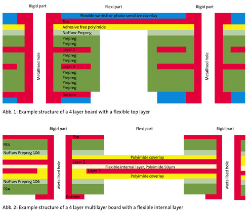
Flexible circuits (sometimes called flexible wires) are etched on the polymer base material on a printed copper or polymer film circuit. For thin and light devices with compact and complex construction, the design solution includes a single path for three-dimensional assembly of a multi-layered complex. The total flexible assembly weight and volume is 70% lower than that of traditional wire rope. Flexible panels can also enhance their strength by using a reinforcement material or a liner for additional mechanical stability. Flexible PCB with higher assembly reliability and flexible circuit board reduces the hardware required for Nellian, such as common solder joints, body, wiring and cables in traditional electronic packages, allowing Flexible panels provide higher assembly reliability and throughput. Because complex systems include traditionally connected hardware in assemblies, a component’s movement rate is highly visible.
In the mass rigid flex PCB production of small electronics (such as small computers), flexible PCBs combined with rigid laminates have become commonplace and cost-optimized. The flexible PCB is equipped with a rigid sheet (such as layer G-10) with a suitable groove position to facilitate later separation. After assembling the parts and the welded wave, the rigid sheet is divided into different sections by cutting it so that it folds into the desired shape. Paper phenolic laminates can be divided into different grades, most can be used at temperatures up to 70 ~ 105, and working for long periods at temperatures above this range may lead to some Performance degraded. And overheating can cause fouls, and in the affected areas the insulation resistance may drop to a very low value. In a high humidity environment, the insulation resistance of the surface will significantly decrease, however, when the humidity decreases, the insulation resistance will increase.
Most of the rigid flex PCB design elements of rigid printed circuit boards have been applied to the design of flexible printed circuit boards. However, there are new factors that need attention. Because the thermal capacity of the flexible printed circuit board is poor (compared to the rigid printed circuit board), adequate wire width should be provided. The principle of line width selection is given when the current exceeds 1A. When several conductors carrying large currents are facing each other or are close together, there is a need for wire width or spacing when considering the temperature concentration issue. Static PCB: should be preferred where possible with a rectangular shape as it can better retain the base material. There should be enough free margins near the edge, depending on the possible excess space of the substrate.
Wire widths are smaller and spacing should be minimized as much as possible. If geometrical space allows, well arranged fine strings should be converted to wide strings. As a general standard, the bending radius should be designed as large as possible. The use of thinner sheets (eg 50μm aluminum foil instead of 125μm copper foil) and the wider wire can improve the ability to bend more cyclic. For a large number of bending cycles, a flexible printed circuit board side usually shows better performance.

Drill to copper – Outer layers: 6 mil
Drill to copper – Inner layers: 8 mil
Copper Thickness: 0.5 oz – 5 oz
Minimum Hole Size: 0.005″
Minimum Trace/Space: 0.003″/0.003″
Minimum Pitch: 0.5 mm
Copper to board edge: 0.007″
Coverlay Opening: 0.003″
Coverlay Web (Kapton): 0.006″
PCBSky is an industry leader in PCB manufacturing with more than 10 years experience. We process single, double-sided, Multi-Layer, and Rigid Flex circuits.If you need any of them, welcome to contact us for the price and datasheet. Have questions about engineering problems or need help with your engineering issues? Not sure who can provide reliable answers to your engineering questions? Just bring your questions to our engineers. Engineering can be a difficult subject for many of our customers, but luckily we’re here to help. Our verified engineers can help you with engineering information and customized answers to all your engineering questions. You can ask any engineering question and get expert answers in as little as 24 hours.