We are a China-based, custom PCB manufacturer with full, in-house manufacturing capabilities. We have been in business since 2011- specializing in quick turn, high quality custom
.Our mission is to provide you with the best service and fabrication in the industry. We offer custom quotes, superior customer service, and on time deliveries. We stand behind our products 100% and take pride in a close and cooperative partnership with our customers.
There is a lot that goes into manufacturing a circuit board. Here is our brief tutorial on the PCB manufacture process.
What does it take to build Printed Circuit Boards?
Introduction to Manufacturing
When it comes to electronics, printed circuit boards are used to mechanically support and electrically connect electronic components using conductive pathways, or traces, etched from copper sheets laminated onto a non-conductive substrate. Alternative names are printed wiring board or PWB or etched wiring board.
Printed circuit boards are rugged, inexpensive, and can be highly reliable. They require much more layout effort and higher initial cost than either wire-wrapped or point-to-point constructed circuits, but are much cheaper, faster, and consistent in high volume production.
The two major stages for manufacturing a PCB are:
- Printed Circuit Board Design
- Printed Circuit Board Manufacturing (PCB Fabrication)
Printed Circuit Board Design
Usually an electronics or electrical engineer designs the circuit, and a layout specialist designs the PCB. The designer must obey numerous
PCB layout guidelines to design a PCB that functions correctly, yet is inexpensive to manufacture.
The Circuit Design
The Circuit Diagram, also called the Schematic or Logic Diagram, maps out the electronics and connections in the most readily readable form. The designer needs to do background work while producing the Circuit diagram, researching specifications of components, interaction between components (especially timing and loading) physical packages, and arrangement of connector pinouts. The circuit will often start on paper and finish in Computer Aided Design (CAD) format. The finished circuit diagram, supported by notes if required, is the main reference document for the design.
Printed Circuit Board Manufacturing Techniques
Electronic Design Automation (EDA)
PCB designers often use electronic design automation to produce a layout. The EDA program stores design information, facilitates editing the design, and can also automate repetitive design tasks.
The first stage is converting the circuit schematic into a net list. The net list is conceptually a list of component pins and the circuit nodes, or nets that each pin connects to. Often the schematic capture EDA program, operated by a circuit design engineer, is responsible for netlist generation, and the netlist is imported into the PCB layout program.
The next step is to decide the position of each device. The easy way to do this is to specify a grid of lettered rows and numbered columns where the devices should go. The computer then assigns pin 1 of each device in the bill of materials to a grid location. Typically, the operator may assist the automated placement routine by specifying rooms, or specific regions of the circuit boards, where certain groups of components should be placed. For example, the parts associated with a power supply subcircuit might be assigned to a region near the power input connector. In other cases devices may be manually placed, either to optimize the electrical performance of the circuit, or to place components such as knobs, switches, and connectors as required by the mechanical design of the system.
The computer then explodes the device list into a complete pin list for the circuit board by using templates from a library of footprints associated with each type of device. Each footprint is a map of a device’s pins, usually with a recommended pad and drill hole layout for each device. The library allows the footprint to be drawn only once, and then shared by all devices of that type.
In some systems, high-current pads are identified in the device library, and the associated nets are flagged for attention by the PCB designer. High current runs require wider traces, and the designer or circuit design engineer usually decides the width.
The computer program then merges the netlist (sorted by pin name) with the pin list (sorted by pin name), transferring the physical coordinates of the pin list to the netlist. The netlist is then resorted, by net name.
Some systems can optimize the design by swapping the positions of parts and logic gates to reduce the length of copper runs. Some systems also automatically discover power pins in the devices, and generate runs or vias to the nearest power plane or conductor.
The programs then try to route each net in the signal-pin list, finding some sequence of connections in the available layers. Often layers are assigned to power and ground, with one layer to vertical, and another to horizontal wires. The power layers shield the circuits from noise.
The routing problem is equivalent to the traveling salesman problem, and is therefore NP complete, and therefore not amenable to a perfect solution. One practical routing algorithm is to pick the pin farthest from the center of the circuit boards, then use a greedy algorithm to select the next-nearest pin with the same signal name.
After automated routing, usually there is a list of nets that must be manually routed.
Once routed, the system may have a series of strategy subroutines to reduce the production cost of the PCB. For example, one routine might remove unneeded vias (each via is a drill hole, and costs money to make). Another might round edges of conductor runs, and widen or move runs apart to maintain safe spacing. Another strategy might adjust large copper areas so that they form nets, or large blank areas may get unconnected “checks” of copper. The nets and checks reduce pollution by extending the life of the etching bath, and speed production by evening-out the copper concentration in the etching bath.
Some systems provide design rule checking to validate the design for electrical connectivity and clearance, rules for circuit board manufacture, assembly and test, heat flow and other errors.
The silk-screen, solder mask, and solder paste stencil(s) are often designed as auxiliary layers.
Finally, the copper layers are then converted to Gerber files, a format of numerical control file for a photoplotter. Historically, an additional aperture file was required to link each numerically designated aperture referred to in the Gerber file with an actual shape to be plotted. Newer Gerber files embed the aperture information in the Gerber file itself. The hole locations are encoded in drill files. The drill files may be sorted to minimize drill-head movement time, and bit changes.
Physical composition
Most PCB are composed of between one and sixteen (or even more) conductive layers separated and supported by layers of insulating material (substrates) laminated (glued) together. Layers may be connected together through drilled holes called vias. Either the holes are electroplated or small rivets are inserted. High-density PC may have blind vias, which are visible only on one surface, or buried vias, which are visible on neither.
Substrates
Low-end consumer grade PCB substrates frequently are made of paper impregnated with phenolic resin, sometimes branded “Pertinax”. They carry designations such as XXXP, XXXPC, and FR-2. The material is inexpensive, easy to machine by drilling, shearing and cold punching, and causes less tool wear than glass fiber reinforced substrates. The letters “FR” in the designation indicate Flame Resistance.
High-end consumer and industrial circuit board substrates are typically made of a material designated FR-4. This consists of a woven fiberglass mat impregnated with a flame resistant epoxy resin. It can be drilled, punched and sheared, but due to its abrasive glass content requires tools made of tungsten carbide for high volume production. Due to the fiberglass reinforcement, it exhibits about five times higher flexural strength and resistance to cracking than paper-phenolic types, albeit at higher cost.
PCB for high power radio frequency (RF) work use plastics with low dielectric constant (permittivity) and dissipation factor, such as Rogers® 4000, Rogers® Duroid, DuPont® Teflon® (types GT and GX), polyimide, polystyrene and cross-linked polystyrene. They typically have poorer mechanical properties, but this is considered an acceptable engineering tradeoff in view of their superior electrical performance.
PCB designed for use in vacuum or in zero gravity, as in spacecraft, being unable to rely on convection cooling, often have thick copper or aluminum cores to dissipate heat from electrical components.
Not all circuit boards use rigid core materials. Some are designed to be very or slightly flexible, using DuPont’s® Kapton® polyimide film, and others. This class of boards, sometimes called flex circuits, or rigid-flex circuits, respectively, are difficult to create but have many applications. Sometimes they are flexible to save space (PCBs inside cameras and hearing aids are almost always made of flex circuits so they can be folded up to fit into the limited available space). Sometimes, the flexible part of the circuit board is actually being used as a cable or moving connection to another board or device. One example of the latter application is the cable connected to the carriage in an inkjet printer. Power electronic applications require low-thermal resist-substrates, with thick copper track to carry high currents. The main technologies are ceramic-based substrates (Direct Bonded Copper) and metal-based substrates (Insulated Metal Substrate).
Manufacturing Technique(s)
Patterning/Imaging
The vast majority of “printed circuit boards” are made by adhering a layer of copper over the entire substrate, sometimes on both sides, (creating a “blank PCB”) then removing unwanted copper after applying a temporary mask (e.g. by etching in ferric chloride), leaving only the desired copper traces. A few PCBs are made by adding traces to the bare substrate usually by a complex process of multiple electroplating.
There are three common methods used for the production of printed circuit boards:
Silk screen printing uses etch-resistant inks to protect the copper foil. Subsequent etching removes the unwanted copper. Alternatively, the ink may be conductive, printed on a blank (non-conductive) board. The latter technique is also used in the manufacture of hybrid circuits.
Photoengraving uses a photomask and chemical etching to remove the copper foil from the substrate. The photomask is usually prepared with a photoplotter from data produced by a technician using computer-aided PCB design software. Laser-printed transparencies are sometimes employed for low-resolution photo plots.
PCB Milling uses a 2 or 3 axis mechanical milling system to mill away the copper foil from the substrate. A PCB milling machine (referred to as a ‘PCB Prototyper’) operates in a similar way to a plotter, receiving commands from the host software that control the position of the milling head in the x, y, and (if relevant) z axis. Data to drive the Prototyper is extracted from files generated in PCB design software and stored in HPGL or Gerber file format.
Lamination
Some PCBs have trace layers inside the PCB and are called multi-layer PCBs. These are formed by bonding together (using high pressure in a press) separately etched thin boards.
Drilling
Holes, or vias, through a PCB are typically drilled with tiny drill bits made of solid tungsten carbide. The drilling is performed by automated drilling machines with placement controlled by a drill tape or drill file. These computer-generated files are also called numerically controlled drill (NCD) files or “Excellon files”. The drill file describes the location and size of each drilled hole.
When very small vias are required, drilling with mechanical bits is costly because of high rates of wear and breakage. In this case, the vias may be evaporated by lasers. Laser-drilled vias typically have an inferior surface finish inside the hole. These holes are called micro vias.
It is also possible with controlled-depth drilling, laser drilling, or by pre-drilling the individual sheets of the PCB before lamination, to produce holes that connect only some of the copper layers, rather than passing through the entire circuit board. These holes are called blind vias when they connect an internal copper layer to an outer layer, or buried vias when they connect two or more internal copper layers.
The walls of the holes, for circuit boards with 2 or more layers, are plated with copper to form plated-through holes that electrically connect the conducting layers of the PCB.
Solder plating and solder resist
The pads and lands to which components will be mounted are typically plated, because the bare copper is not readily solderable. Traditionally, any exposed copper was plated with solder. This Printed Circuit Board Press
Press used in manufacturing custom printed circuit boards.
solder was traditionally a tin-lead alloy, however new solder compounds are now used to achieve compliance with the RoHS directive in the EU, which restricts the use of lead. Edge connectors, made on the sides of some circuit boards, are often gold plated. Gold plating is also sometimes applied on the whole boards.
Areas that should not be soldered to may be covered with a polymer solder resist coating. The solder resist prevents short circuits between nearby component leads.
Silk screen
Line art and text may be printed onto the outer surfaces of a PCB by silk screening. When space permits the silk screen text can indicate component designators, switch setting requirements, test points, and other features helpful in assembling, testing, and servicing circuit boards. In one sided PCBs, silk screen is also known as the ‘red print’.
Populating
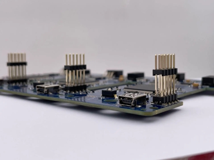
In through-hole construction, component leads may be inserted in holes and electrically and mechanically fixed to circuit board with a molten metal solder. In surface-mount construction, the components are simply soldered to pads or lands on the outer surfaces of the PCB. Often through-hole and surface-mount construction must be combined in a single PCB because some required components are available only in surface-mount packages, while others are available only in through-hole packages.
Test and validation
Unpopulated boards may be subjected to a bare-board test where each circuit connection as defined in a netlist is verified as correct on the finished board. For high-volume production, a Bed of nails tester or fixture is used to make contact with copper lands or holes on one or both sides of the board to facilitate testing. A computer will instruct the electrical test unit to send a small amount of current through each contact point on the bed-of-nails as required, and verify that such current can be seen on the other appropriate contact points. For small- or medium-volume circuit boards, flying-probe testers use moving test heads to make contact with the copper lands or holes to verify the electrical connectivity of the board under test.
Protection and packaging
PCBs intended for extreme environments often have a conformal coat, which is applied by dipping or spraying after the components have been soldered. The coat prevents corrosion and leakage currents or shorting due to condensation. The earliest conformal coats were wax. Modern conformal coats are usually dips of dilute solutions of silicone rubber, polyurethane, acrylic, or epoxy. Some are engineering plastics sputtered onto the PCB in a vacuum chamber. Mass-production PCBs have small pads for automated test equipment to make temporary connections. Sometimes the pads must be isolated with resistors.
PCB Manufacturing Departments
Engineering and Cam Area