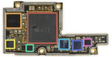
SLP (substrate like PCB) is the next generation of PCB board. It can shorten the line width / line distance from 40 / 50 microns of HDI to 20 / 35 microns, that is, the minimum line width / line distance will be shortened from 40 microns of HDI to less than 30 microns of SLP. At present, SLP can achieve 25 microns. In terms of manufacturing process, SLP is closer to IC carrier used in semiconductor packaging, but it has not yet reached the specification of IC carrier, and its purpose is still to carry various active and passive components, so it still belongs to the category of PCB. SLP board for smart phones can carry twice as many electronic components as HDI in the same area.
Due to the development trend of smart phones, tablet computers, wearable devices and other electronic products towards intelligence, miniaturization and functional diversification, the number of components to be carried on PCB has increased significantly, but the required size, weight and volume are shrinking. In this context, the requirements of PCB wire width, spacing, micro disk diameter and hole center distance, as well as the thickness of conductor layer and insulation layer are decreasing, while the traditional HDI is limited by the manufacturing process. Therefore, SLP technology with more stacking layers, smaller line width and line spacing and more functional modules becomes the inevitable choice to solve this problem.With the same function of PCB, SLP can greatly reduce the area and thickness of HDI board, the thickness is reduced by about 30%, and the area is reduced by about 50%, which can make more space for electronic products to develop new hardware or increase battery capacity.
3. SLP Technology
SLP is suitable for SIP packaging technology. One of the major improvement directions of SLP requirements is its compliance with SIP packaging technology. SIP (system in a package) is a system level packaging technology defined by the international semiconductor route organization (ITRS), which is a single standard package with multiple active electronic components and optional passive devices with different functions, such as processor, memory, MEMS and other functional chips and optical devices, etc., which are integrated into one package to achieve certain functions, Thus, it can realize a basic and complete function and form a package technology of a system or subsystem.
There are two ways to realize the functions of electronic whole system, including SOC (system on chip) and sip package. SOC refers to the integration of IC with different functions into a chip to realize the electronic whole system. In recent years, due to the increasing difficulty of semiconductor process, SoC development has encountered technical bottleneck, SIP has become a new industrial technology trend in electronic industry. For SIP, because the density of the internal wiring of system level packaging is very high, the ordinary PCB board is difficult to carry, and SLP is more suitable for the density requirements, and it is suitable for SIP packaging carrier.
By Application
· Consumer Electronics
· Computing And Communications
· Automotive
· Medical
· Industrial
· Military, Defense, And Aerospace
· By Inspection Technology
· Automated Optical Inspection (AOI)
· Direct Imaging (DI) Or Laser Direct Imaging (LDI)
· Automated Optical Shaping (AOS)
4. SLP manufacturing technology
At present, there are three main technologies in the
PCB manufacturing process and carrier board, including reduction method, full addition method and semi addition method
Reduction method: reduction is the first traditional PCB technology, and also a mature manufacturing process. Generally, photosensitive anti-corrosion materials are used to complete the graphic transfer, and the material is used to protect the areas without etching removal. Then, the copper layer in unprotected areas is removed by acid or alkaline etching potions.
SAP: the total addition process adopts the insulating substrate with photosensitive catalyst. After exposure according to the line graph, the conductor figure is obtained by selective chemical deposition of copper.
MSAP: the semi addition method is based on how to overcome the problems of reduction and addition in fine line production. The semi addition method is used to make chemical copper on the substrate and form the anti-corrosion graph on it. After electroplating process, the graph on the substrate is thickened, the anti-corrosion graph is removed, and then the excess chemical copper layer is removed by flash etching. The area that is protected by dry film without plating thickening is removed quickly during differential etching, and the reserved part forms a circuit.
SLP belongs to PCB, but its line width / line distance is 20 from the view of manufacturing process μ m/35 μ m. It is impossible to use reduction method, and MSAP process technology is also required.