
Printed circuit board (PCB) is a structural component composed of insulating material and conductor wiring. When the final product is manufactured, it will be equipped with integrated circuits, transistors, dipoles, passive components (such as resistors, capacitors, connectors, etc.) and various other electronic components. By means of wire connection, electronic signal connection and corresponding functions can be formed.
Because the printed circuit board of HDI PCB factory is not a general terminal product, the definition of its name is somewhat confused. For example, the mother board for personal computers is called the motherboard, which cannot be called the circuit board directly. Although there are circuit boards in the motherboard, they are not the same. Therefore, when evaluating the industry, they are related but cannot be said to be the same. For example, because the integrated circuit parts are loaded on the circuit board, the news media call him IC board, but in essence, it is not the same as printed circuit board.
Under the premise that electronic products tend to be multi-functional and complex, the contact distance of integrated circuit elements will be reduced, and the speed of signal transmission will be relatively increased. Accordingly, the number of connections will be increased, and the length of inter-point wiring will be shortened locally. These require HDI PCB factory to use high-density line configuration and microporous technology to achieve their goals. Wiring and spanning are basically difficult to achieve for single and double panels, so PCB will move towards multi-layer, and because of the increasing number of signal lines, more power and ground layers are the necessary means of design. All of these make the Multilayer Printed Circuit Board more common.
For the electrical requirements of high-speed signals, the circuit boards produced by HDI PCB factory must provide impedance control with AC characteristics, high-frequency transmission capability, and reduce unnecessary radiation (EMI). With the structure of stripline and Microstrip, multi-layer design becomes necessary. In order to reduce the quality of signal transmission, insulating materials with low dielectric coefficient and low attenuation rate will be used. In order to cooperate with the miniaturization and array of electronic components, the density of circuit boards will be continuously increased to meet the demand. The emergence of BGA (Ball Grid Array), CSP (Chip Scale Package), DCA (Direct Chip Attachment) and other parts assembly modes has pushed PCB forward to an unprecedented high density.
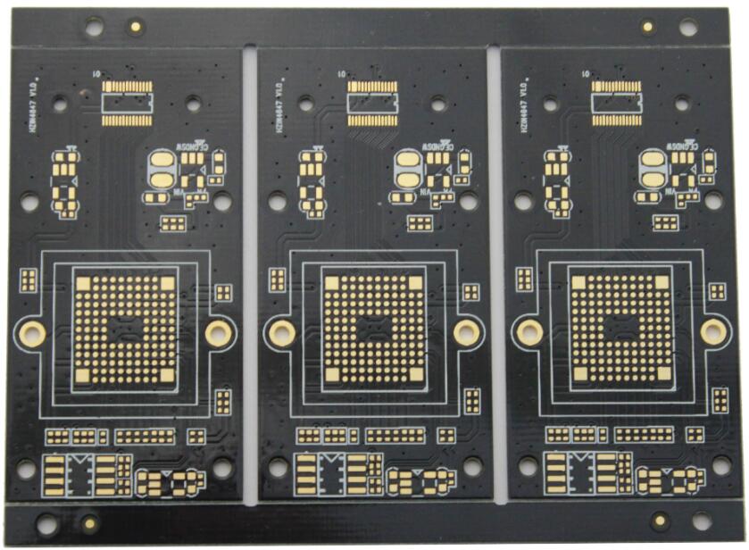
All holes less than 150 um in diameter are called micro via in the industry. Circuits made by using the geometric structure technology of micro holes can improve the efficiency of assembly, space utilization and so on. At the same time, it is necessary for miniaturization of electronic products.


