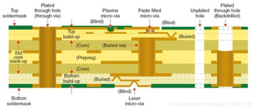
Via is one of the most important parts of PCB, and the cost of drilling usually accounts for 30% to 40% of PCB board making cost. From the design point of view, a via is mainly composed of two parts, one is the middle drill hole, the other is the pad area around the drill hole. The size of these two parts determines the size of the via.
Obviously, in high-speed and high-density PCB design, designers always hope that the smaller the via is, the better, so that there can be more wiring space on the board. In addition, the smaller the via is, the smaller its parasitic capacitance is, which is more suitable for high-speed circuits.
However, the decrease of hole size brings the increase of cost, and the size of through-hole can not be reduced without limit. It is limited by drilling and plating technology: the smaller the hole is, the longer the drilling time is, and the easier it is to deviate from the center position; and when the depth of the hole is more than 6 times of the diameter of the hole, the uniform copper plating on the hole wall cannot be guaranteed.
Therefore, we need to consider the following issues in comprehensive design and production.
A.In principle, the inner diameter of the through via hole should be 0.2mm (8mil) and above, and the outer diameter should be more than 0.4mm (16mil). If there is any difficulty, it must be controlled within the outer diameter of 0.35mm (14mil);
According to the experience, the inner diameter and outer diameter of PCB common via size generally follow x * 2 ± 2mil (X represents inner diameter). For example, 8 / 14 mil, 8 / 16 mil or 8 / 18 mil can be designed for 8 mil inner diameter vias; for example, 12 / 22 mil, 12 / 24 mil, 12 / 26 mil vias can be designed for 12 mil.
B.If BGA pin pitch is 0.65mm or above, it is recommended not to use blind hole, and the cost will be greatly increased.
The first-order blind hole (top layer-l2 layer) is generally used when blind hole is used. The inner diameter of through hole is generally 0.1mm (4mil) and the outer diameter is 0.25mm (10mil).
C.Vias cannot be placed on pads smaller than 0402 resistance capacitance pad;
Theoretically, the inductance of the lead wire placed on the pad is small, but during the production, the solder paste is easy to go into the via hole, resulting in uneven solder paste, resulting in the phenomenon of device standing up. The recommended spacing is 4-8 mil.
D.The distance between via hole and via hole should not be too close, and the via hole is easy to be broken.
Generally, the via spacing is 0.5mm and above, 0.35mm-0.4mm is strictly avoided, and 0.3mm or below is prohibited.
E.In addition to the thermal vias, the vias less than 0.5mm need to be plugged and covered with soldermask (the inner diameter is 0.4mm and the hole needs to be plugged).
1) Especially for the device with metal shell, the vias should not be drilled under the main body, but a certain plug hole of vias should be drilled to cover oil, so as to avoid short circuit between the shell and vias.
2) According to the production feedback of
PCB factory, it is often mentioned that via under BGA is too close to the pad and via needs to be moved.
This situation is caused by the fact that via is not equidistant from BGA pad. At present, it is normal that via and test hole under BGA are not equidistant from each pad of BGA. PCB designers do not pay attention to this, which leads to continuous engineering problems and a hidden danger to welding quality.
Therefore, we directly recommend drilling to the center of the two pads, especially in BGA. Due to the small pitch distance in BGA, the through hole plug hole under BGA needs to be covered with oil after drilling, so as to avoid short circuit of BGA Solder ball.F.The fixed pads of earphone terminals, keys,
flex PCB, etc. are designed to prevent the copper skin from falling off. If conditions permit, the pad can drill 1-2 via holes (the vias are evenly placed), which can effectively improve the “fixation”.