PCI Express (peripheral component interconnect express) is a high-speed serial computer extension bus standard. Its original name is “3gio”. It was proposed by Intel in 2001 to replace the old PCI, PCI-X and AGP bus standards. PCIe is a high-speed serial point-to-point dual channel high bandwidth transmission. The connected device allocates exclusive channel bandwidth and does not share bus bandwidth. It mainly supports active power management, error reporting, end-to-end reliable transmission, hot swap and quality of service (QoS) functions. The name of “PCI Express” was changed to “PCI-Express” after PCI-sig (PCI special interest organization) certification and release. Its main advantage is its high data transmission rate. The highest version of 16x 2.0 can reach 10Gb / s, and it has considerable development potential. PCI Express also has a variety of specifications, from PCI Express 1x to PCI Express 32x, which can meet the needs of low-speed and high-speed devices in the future. The latest interface of PCI Express is the PCIe 3.0 interface. Its bit rate is 8GB / s, which is about twice the bandwidth of the previous generation products. It also includes a series of important new functions, such as transmitter and receiver equalization, PLL improvement and clock data recovery, to improve data transmission and data protection performance. Intel, IBM, LSI, OCZ, Samsung (under plan), SanDisk, STEC, Super Talent and Toshiba (under planning). For the massive data growth, users can apply to larger and more scalable systems. With the addition of the latest LSI MegaRAID controller and the excellent performance of HbAS, greater system design flexibility can be achieved. Of course, mainstream motherboards can support PCI Express 1.016x, and some higher end motherboards can support PCI Express 2.016x.
PCIe standard
A PCI Express card is suitable for its physical size or larger slot (use x 16 as the largest), but may not fit into a smaller PCI Express slot; for example, an x 16 card may not fit into a × 4 or × 8 slot. Some slots use open sockets to allow physically longer cards and negotiate optimal electronic and logical connections.
The number of channels actually connected to the slot may also be less than supported by the physical slot size. An example is that a card with x 1, x 2, x 4, x 8 and x 16 can be run in an x 16 slot, and only four channels are provided when the card is running. Its specification can be read as “× 16 (× 4 mode)”, and the symbol “× size @ × speed” (“× 16 @ × 4”) is also common. The advantage is that such a slot can accommodate a larger range of PCI Express cards without requiring motherboard hardware to support full transfer rate.
The card itself is designed and manufactured in various sizes. For example, solid state drives (SSDs) in the form of PCI Express cards usually use HHHL (half height, half length) and FHHL (full height, half length) to describe the physical size of the card.
1. The length of wiring from the gold finger edge of PCB to the pin of PCIe chip should be limited to 4 inches (about 100 mm).
2. The perm / N, PETP / N and peckp / N of PCIe are three differential pairs. Pay attention to the protection (the distance between differential pairs, the distance between differential pairs and all non PCIe signals is 20MIL) to reduce the influence of harmful crosstalk and electromagnetic interference (EMI). High frequency signal line should be avoided on the reverse side of chip and PCIe signal line, and full GND is preferred).
3. The length difference of the two routing lines in differential alignment is 5MIL at most. Each part of the 2 routes requires length matching. The line width of differential impedance line is 7mil, and the distance between two lines in differential pair is 7mil.
4. When changing the layer of PCIe signal pair routing, ground signal vias should be placed near the signal pair vias, and 1 to 3 ground signal vias are recommended for each pair of signals. The PCIe differential pair adopts 25 / 14 vias, and the two vias must be placed symmetrically.
5. The two AC coupling capacitors of differential pair must have the same package size, and the position should be symmetrical and placed close to the golden finger. The recommended capacitance value is 0.1uF.
6. The signal lines such as SCL cannot pass through the main chip of PCIe.
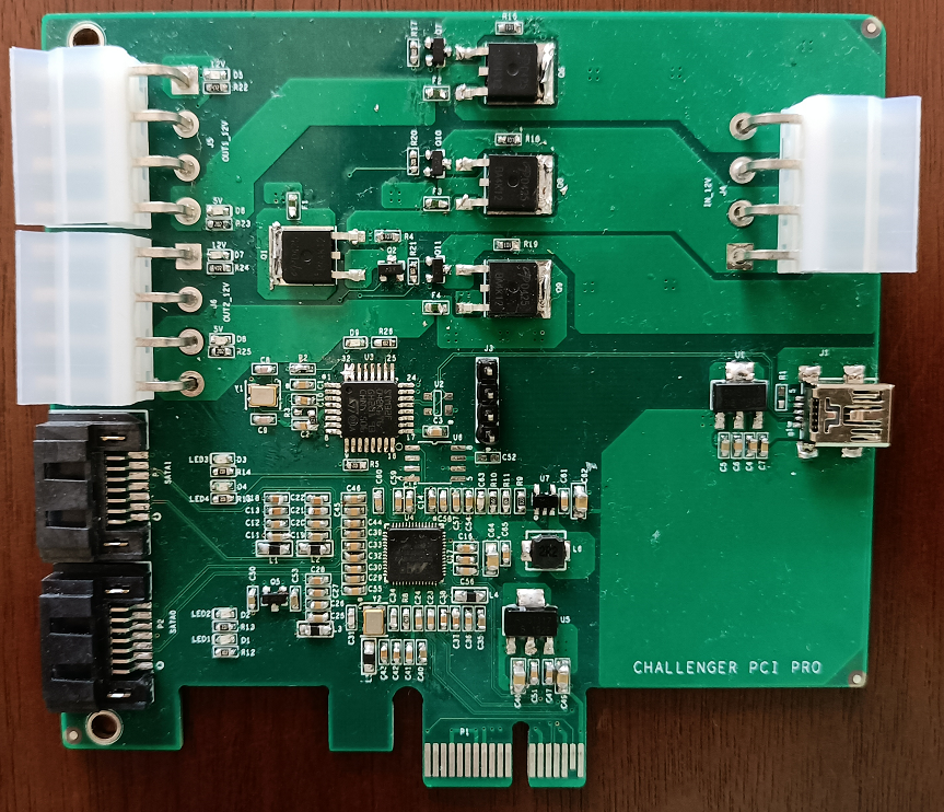
The above figure is the product of PCIe designed by our company. If you have the same requirement, please contact us.