“Plating Over Filled Via” (POFV) and “Via in Pad Plated Over” are two different concepts in printed circuit board (PCB) design, both involving vias and metallization of the PCB, but with some differences. Here are the similarities and differences between them:
Similarities:
Metallization Treatment: Both involve covering vias on the PCB with a metal layer, typically copper, to achieve electrical connections.
Purpose: They are both used to enhance the electrical performance of the PCB, including signal transmission, heat dissipation, and connections.
Technical Requirements: Both require special PCB manufacturing techniques and processes, often requiring high precision manufacturing and processing.
Differences:
Concept: The concepts of the two are different.
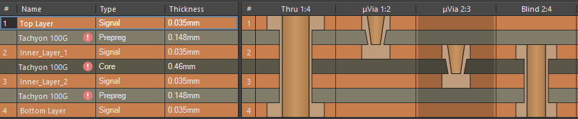
“Plating Over Filled Via” (POFV) refers to vias that are filled with a dielectric or other material, and then metallized on top of and around the filled material to create electrical connections.
“Via in Pad Plated Over(VIPPO)” refers to vias that are located within solder pads, and are metallized above and around the pad to allow for direct component soldering to that pad.
Applications:
POFV is typically used in cases where even current distribution needs to be created on the PCB to reduce signal distortion.
“Via in Pad Plated Over” is commonly used in surface mount technology, allowing pins or balls of electronic components to directly connect to the solder pad, often used in BGA (Ball Grid Array) packaging.
Physical Location:
POFV involves vias located in non-pad areas of the PCB, primarily aimed at improving current distribution.
“Via in Pad Plated Over” involves vias located within solder pads, so that the pins or balls of components can connect to the pad.
In summary, while both concepts involve metallization treatment and vias on the PCB, their primary applications and concepts are different. The choice of which technique to use depends on the specific PCB design requirements and application scenarios.