
Digital devices are developing towards the direction of high speed, low consumption, small size and high anti-interference, which development trend puts forward many new requirements for the design of high frequency PCB. Based on years of experience in hardware design, the author summarizes some rules of arrangement of high frequency PCB components.
Rules of arrangement of high frequency PCB components.
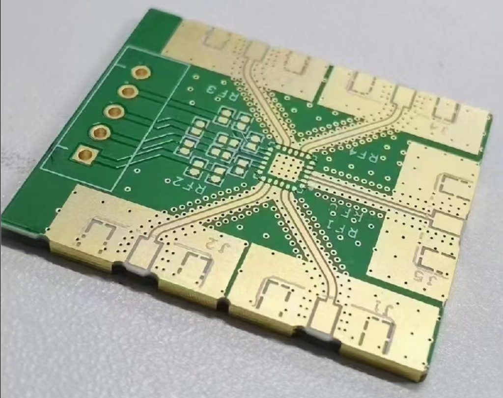
1) Under normal conditions, all components should be arranged on the same surface of the printed circuit. Only when the top layer is too dense, some devices with limited height and small heat output, such as patch resistance, patch capacitance and patch IC, can be placed on the bottom layer.
2) On the premise of ensuring the electrical performance, the components shall be placed on the grid, parallel or perpendicular to each other, so as to be neat and beautiful. In general, the components are not allowed to overlap; The elements should be arranged compactly and the input and output elements should be kept as far away as possible.
3) There may be a high potential difference between a component or a wire, should increase their distance, so as not to discharge, breakdown and cause unexpected short circuit.
4) Components with high voltage should be placed where it is not easy to reach by hand during debugging.
5)The component located at the edge of the plate should be at least 2 thickness away from the edge of the plate.
6) Components shall be evenly distributed and uniformly spaced throughout the board.


