
In order to make the design of high frequency printed circuit board more reasonable and the anti-interference performance better, many high frequency PCB companies should consider the following aspects in the design of high frequency printed circuit board.
1. Using the middle inner plane as power supply and wire layer can shield, reduce parasitic inductance, shorten the length of signal line and reduce cross-interference between signals.
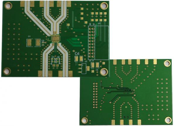
2. The route must be turned at 45 degrees, which can reduce the transmission of high frequency signals and the coupling between them.
3. The shorter the line length, the better the parallel distance between the two lines.
4. The smaller the number of holes, the better.
5. Interlayer wiring direction should be vertical, that is, the top layer is horizontal, and the bottom layer is vertical, which can reduce the interference between signals.
6. Increasing the copper cladding on the ground can reduce the interference between signals.
7. Packet processing of important signal lines can significantly improve the anti-jamming ability of the signal. Of course, it can also process the jammer in packet so that it cannot interfere with other signals.
8. Signal routing cannot be circular. It needs to be routing according to chrysanthemum chain.
9. Decoupling capacitance. The decoupling capacitor is connected across the power section of the integrated circuit.
10. High-frequency choke devices should be connected when connecting public ground wires digitally and analogically, usually high-frequency ferrite beads with central holes through wires.
PCBSky is a high frequency PCB company worthy of your trust. Welcome to order.


