
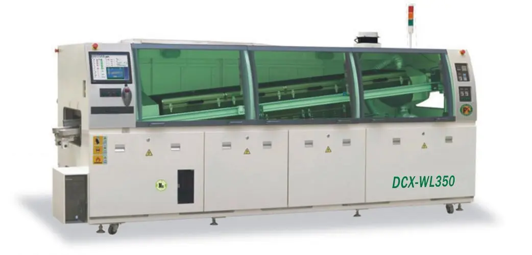
Wave Soldering is the process of soldering through hole components onto a PCB by passing the exposed leads of the components placed on a board over a wave of molten solder. The solder wave flows under the PCB board and applies solder to the leads of components placed on the PCB board. It is primarily used to solder thru hole components on printed circuit boards. It is not usually used to solder surface mount components. If you are looking to solder surface mount components on a PCB, then other soldering processes like reflow soldering can be used.
Wave soldering was developed in 1956. At the time most components were soldered by hand which was very tedious and time consuming. The idea to pass a PCB board over a wave of molten solder seemed like a good one, and worked well as most/all components at the time were through-hole components with very long leads.
The Wave Soldering Process Consists of four main steps:
Step 1: Applying Flux
Solder flux is a chemical cleaning agent used when soldering electronic components onto printed circuit boards. It is applied to the board to help avoid oxidation of the copper traces when exposed to air. It is a very important process that is required to ensure that the PCB board operates in a reliable and consistent manner. In the case of wave soldering, Flux is applied to the bottom of the board before the PCB is sent through solder wave.
Step 2: Preheat
Once flux has been applied to the PCB. It is important to heat the underside of the board to a temperature of about 80 – 100 degrees Celsius. This allows any solvents present in the flux to evaporate. The flux applied using any method, is mixed with a solvent to make the application process easier, as the solvent reduces the viscosity of the flux. The flux without the solvent is a very sticky substance. This solvent is usually some volatile organic compound, which is flammable. This requires the removal of the solvent before the underside of the board comes into contact with the very hot solder wave. This is why the entire board is put through a preheating stage so as to minimize the chances of the PCB setting itself on fire.
During the pre-heat phase, the fluxed board is passed over an array of infra-red heaters. These heaters have a heat-reflecting panel behind them. A gentle gust of air is blown between the boards and the heaters. This increases the rate of removal of solvent laden air. The heat-reflecting panel behind the heater not only reflects heat but also conserves thermal energy by reducing the temperature differential between the under-side and the top of the board.
Step 3: The Solder Wave
The Printed Circuit Board is then passed through a Solder Wave. To ensure a good connection, molten solder must impact the board with maximal kinetic energy. This can be achieved when the solder wave meets the leads of the through hole components just as it is about to crest. The crest of a wave is the highest point of it.
The solder wave covers the leads of all the through hole components and connects them to the PCB.
A Solder-wave is produced by forcing molten solder-upwards through a vertical conduit. This wave of molten solder eminates from a vertical conduit, which is called a wave-nozzle. This wave-nozzle is made of narrow slots arranged at right angles to each other. An axial impeller, driven by a variable speed motor is used to drive the solder upwards.
The wave is created by melting solder ingots in a wave tank. The depot of molten solder is maintained at a temperature of about 250 degree Celsius. This has been universally accepted as the standard temperature for maintaining molten solder. If any new type of solder is being used, the temperature of the solder bath would have to change, this is because the efficiency of the a flux is strongly temperature dependent.
Step 4: Cooldown
After the PCB passes over the molten solder wave, the board needs to cool down so that the solder joints can be formed. It is important to maintain a gradual temperature gradient when cooling the PCB after the wave soldering process. The temperature gradient for cooling is selected such that sudden solidification of the solder joints do not crack. This cooling rate/gradient should be selected to reduce thermo-mechanical forces generated on the board due to temperature differentials. This even cooling may be achieved by circulating cold air with zero oxygen content. This colder air must also follow a gradient of cooling proportional to the gradient of cooling which has to be induced on the board and the components on it.
Wave soldering was a very celebrated process at the time of its invention. This was due to high throughput, volume capabilities of this process. However, over time, as technology advanced and components / boards became smaller, surface mount components started to replace Thru-Hole components. This resulted in the need for different soldering processes such as reflow soldering.
Wave soldering is still used today. There are a number of cases where we need to use through hole components and this soldering process is still very common.


