The
PCB silk screen layer is the top layer in the PCB and is generally used for annotations. The correct principle for the layout of the characters on the silk screen layer is: “no ambiguity, stitches at a glance, beautiful and generous”. This is to facilitate
PCB assembly and maintenance, etc., to print the required logo patterns and text codes on the upper and lower surfaces of the PCB.
The silk screen layer in PCB includes Top Silkscreen (top layer), Bottom Silkscreen (bottom layer). That is, the top and bottom layers of the
printed circuit board.
Specification and requirement of PCB screen printing
1. All components, mounting holes and positioning holes have corresponding silk screen marks. In order to facilitate the installation of finished boards, all components, mounting holes and positioning holes have corresponding silk screen marks. H1 and H2 are used for silk screen printing of mounting holes on PCB.
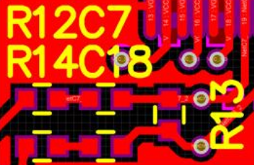
2. The silk screen characters shall follow the principle of left to right and bottom-up, and the principle of left to right and bottom-up shall be followed as far as possible. The direction of electrolytic capacitors, diodes and other polarity devices shall be kept in the same direction in each functional unit.
3. There is no screen printing on the device pad and the tin channel to be tinned, and the device tag number should not be blocked by the device after installation. (high density, except those without screen printing on PCB)
4. In order to ensure the welding reliability of the device, there is no silk screen printing on the solder pad of the device; in order to ensure the continuity of the tin coating, there is no silk screen printing on the tin coating; in order to facilitate the device insertion and maintenance, the device tag number should not be blocked by the device after installation; the silk screen should not be pressed on the through-hole and pad, so as to avoid the loss of part of the silk screen and affect the training when the solder mask window is opened. The screen printing distance is more than 5MIL.
5. The polarity of the components with polarity is clearly indicated on the silk screen, and the polarity direction mark is easy to identify.
6. The number of sheets of PCB photo drawing file is correct, each layer should have correct output and complete layer number output.
7. The device identifier on PCB must be consistent with the identification symbol in BOM list.
8. The direction of the connector with direction is clearly indicated on the silk screen.
9. There should be barcode position identification on PCB. If the space of PCB board is allowed, there should be 42*6 barcode screen frame on PCB. The position of barcode should be considered to facilitate scanning.
10. The screen printing position of PCB board name, date and version number should be clear. The PCB file should have the board name, date, version number, etc. on the board information screen printing, the position is clear and eye-catching.
11. The PCE must have complete relevant information of the manufacturer and anti-static label.Lots of customers come to buy PCB. We keep All types of PCB material in stock, if you need any of them, welcome to contact us for the price and datasheet.