
In today’s fast-paced technological landscape, the Internet of Things (IoT) has emerged as a transformative force, connecting devices, sensors, and systems to enhance convenience, efficiency, and data-driven decision-making. At the heart of this revolution lies the IoT PCB, a specialized printed circuit board that plays a pivotal role in enabling seamless communication and functionality within the IoT ecosystem. In this article, we unravel the concept of IoT PCBs, explore their significance, applications, and shed light on their role in shaping the future of connected devices.
Understanding IoT PCBs
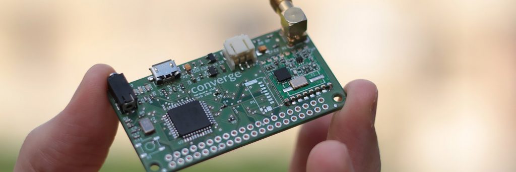
An IoT PCB, also known as an Internet of Things PCB, is a circuit board optimized for the unique demands of IoT devices. These devices often require a combination of compact design, energy efficiency, and the ability to accommodate a diverse range of sensors, processors, and wireless communication modules.
Key Attributes of IoT PCBs
Applications of IoT PCBs
IoT PCBs power a range of smart home devices, including smart thermostats, security cameras, door locks, and lighting systems. These devices can be controlled remotely and can interact with each other to create a cohesive smart home ecosystem.
IoT PCBs are integral to wearable devices like fitness trackers, smartwatches, and health monitors. These devices collect data on users’ activity levels, heart rate, and other health metrics, contributing to a healthier lifestyle.
IoT PCBs are at the heart of industrial IoT (IIoT) applications. They enable real-time data collection, predictive maintenance, and remote monitoring of machinery and processes, enhancing operational efficiency and reducing downtime.
IoT PCBs play a role in precision agriculture by enabling the collection of data from sensors placed in fields. This data informs decisions about irrigation, fertilization, and pest control, optimizing crop yield.
IoT PCBs are used in medical devices like remote patient monitoring systems, pill dispensers, and telehealth platforms. These devices enable healthcare professionals to remotely monitor patients and provide timely interventions.
Benefits of IoT PCBs
IoT PCBs serve as the backbone of the Internet of Things, enabling devices to communicate, collect data, and provide intelligent insights. Designed to cater to the unique demands of IoT applications, these specialized circuit boards embody compactness, energy efficiency, wireless connectivity, and sensor integration. The applications of IoT PCBs span across various sectors, from smart homes and wearables to industrial automation and healthcare. As the IoT ecosystem continues to expand and evolve, IoT PCBs are poised to remain at the forefront, driving innovation, connectivity, and efficiency in the devices that power our connected future.


