Recently, we encountered a PCB leakage problem. The cause is a low-power product. The current of UA level of the whole machine was aged at room temperature for a period of time. After using it for a period of time, it was found that the power consumption of individual sample machines even reached Ma level. Carefully ruled out the problem of components, and finally found a 5V voltage point, in the dormant state of the product should be 0V, but it has a voltage drop of about 1.8V! After patiently cutting the PCB circuit, I was surprised to find that two vias without electrical connection on the PCB could test the resistance value of hundreds of Ohm between each other. Check the original design, two-layer PCB, via hole spacing > 6mil, pad spacing > 18mil, such a design in the PCB industry is a common drilling technology. Wash away the ink, eliminate the ink or the surface layer of the impurity conductive problem, the measured via-hole resistance still exists! After a period of time, I found that it was the “CAF effect” that caused the leakage problem!
What is CAF effect
CAF, fully known as conductive anode filament , refers to the leakage behavior of copper and copper salt in PCB during the migration of copper ions from anode (high voltage) along the microcrack channel between glass fiber wires to cathode (low voltage).
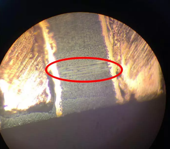
As shown in the following picture, two adjacent vias are longitudinally ground and magnified by 100 times under an electron microscope. The plate is in a dark color, and the bright gold part is copper. It can be seen that there are copper dots and copper wires between the two vias.
The mechanism of CAF is as follows
1. The conventional FR4 PCB is made of glass fiber woven into glass cloth and then coated with epoxy resin. The adhesion between the resin and the glass fiber is insufficient or the adhesive property is poor when the resin is immersed. In addition, in the process of drilling and other mechanical processing, due to the effect of tangential tension and longitudinal impact force, the adhesion force of the resin is further damaged, which may cause the glass fiber bundle to be stretched or separated, resulting in gaps. In the high temperature and humidity environment, the adhesion between epoxy resin and glass fiber is more deteriorated, which promotes the chemical hydrolysis of silane coupling agent on the glass fiber surface, and forms a path for electron migration along the glass fiber reinforced material;
2. Based on the above conditions, if there is a potential difference between the two vias near each other, the copper on the anode with higher potential will be oxidized into copper ion, and the copper ion will migrate to the cathode with lower potential under the action of electric field. In the process of migration, it will combine with impurity ions or Oh – in the board to form water-insoluble conductive salt, which will be deposited between the two insulating holes The electrical distance of the electric gap drops sharply, and even can be directly connected to form a short circuit.
Anode:
Cu → Cu2++2e–
H2O → H++OH-
Cathode:
2H++2e– → H2
Cu2++2OH– → Cu(OH)2
Cu(OH)2 → CuO+H2O
CuO+H2O → Cu(OH)2 → Cu2++2OH–
Cu2++2e– → Cu
Before I realized the bad effect caused by CAF effect, I was surprised by the resistance value between the two vias which were insulated from each other. After consulting the data, I found that many peers had been troubled by this problem. Even CAF effect has been one of the most popular reliability problems in PCB industry!
How to prevent or reduce the occurrence of CAF?
1. Improve the anti CAF ability of base material. For the PCB base material process, it can be improved by improving the ion purity of the material, using low moisture absorption resin, fully soaking glass cloth with resin and combining well. For application side engineers, CAF resistant base material can be considered when selecting base material. Caf resistant base materials can be selected from the following plate selection benefits of base material suppliers.
2. PCB mechanical drilling or laser burning will produce high temperature, exceeding base The TG point of material will melt and form residue. These residues attached to the hole wall will cause poor contact during copper plating. Therefore, slag removal must be carried out before copper plating. Immersion treatment in the slag removal operation will cause certain erosion to the via hole and may lead to copper penetration, which makes the subsequent copper migration easier;
3. In
PCB design, increase the through-hole spacing. In addition, since CAF channels are generated along the same glass fiber bundle, it is helpful to reduce the occurrence of CAF by publishing adjacent through holes;
4. Clean the surface of PCBA, such as dust cleaning with high-pressure air gun, to avoid unnecessary impurity electrolysis caused by impurity residue. In addition, coating three proofing paint on PCBA surface to avoid water vapor invasion, especially in high temperature and high humidity geographical environment.