Designing PCBs (Printed Circuit Boards) with Ball Grid Array (BGA) electronic components presents unique challenges and considerations due to the compact and densely packed nature of BGAs. Here’s an overview of the key points to keep in mind when designing PCBs with BGAs:
- Component Selection: Choose BGAs based on the specific requirements of your project. Consider factors like package size, pin count, ball pitch, and thermal characteristics. Ensure that the selected BGAs are readily available and compatible with your design.
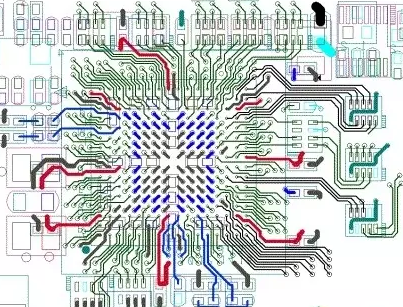
- PCB Layer Stack-up: Carefully plan the layer stack-up of your PCB. BGAs often require additional signal and power layers to accommodate the routing of numerous traces and vias. A typical BGA design may include signal, ground, and power planes.
- Pad Layout: Pay special attention to the BGA pad layout. Ensure that the pad size, shape, and pitch match the specifications provided in the component’s datasheet. Precise placement is crucial to maintain solderability and minimize short circuits.
- Thermal Management: BGAs can generate significant heat, especially in high-performance applications. Incorporate thermal vias and heat sinks, if necessary, to dissipate heat and prevent overheating of the BGA components.
- Routing Constraints: The dense arrangement of BGA balls necessitates careful routing. Utilize trace escape patterns, such as dogbone, via-in-pad, or microvia, to efficiently route signals from the BGA to other parts of the PCB.
- Signal Integrity: Maintain controlled impedance and ensure signal integrity. Signal traces should be of uniform length to prevent skew, and signal integrity analysis tools can help optimize trace widths and spacing.
- Design Tools: Employ PCB design software that supports BGA layouts and provides advanced routing features. These tools can help you visualize, manage, and route the complex interconnections of BGAs.
- Via Placement: Strategically place vias to manage the transition from the BGA to inner layers. Via structures should be designed to minimize signal reflections and crosstalk.
- Manufacturability: Collaborate closely with your PCB manufacturer. Ensure that they are capable of handling BGAs and can meet the specific requirements of your design, including controlled impedance and tight tolerances.
- Assembly and Soldering: Choose an appropriate soldering process, such as reflow soldering, and ensure that the PCB design aligns with the assembly process. Proper solder mask application and stencil design are essential for successful BGA soldering.
- X-ray Inspection: Implement quality control procedures, including X-ray inspection, to verify the integrity of BGA solder joints. This step is critical to detect any soldering defects that may not be visible to the naked eye.
- Testing and Validation: After assembly, conduct thorough functional testing and validation to ensure the BGA components are functioning correctly and reliably.
Designing PCBs with BGA components requires meticulous planning, precise layout, and close collaboration with component suppliers and PCB manufacturers. With the right design tools, expertise, and quality control measures, you can successfully integrate BGAs into your electronic products while meeting performance and reliability requirements.
If you have PCB with BGA and need to design and layout, please contact us.