
First of all, ounces (oz) itself is a unit of weight. The conversion formula of ounces and grams (g) is 1oz ≈ 28.35g.
In the PCB industry, 1oz means the thickness of copper with a weight of 1oz evenly spread over an area of 1 square foot (ft2). It represents the average thickness of copper foil by the weight per unit area. Expressed by the formula, that is, 1oz = 28.35g/ft2 (ft2 is square foot, 1 square foot = 0.09290304 square meter).

Specifically, the conversion method between length and thickness is as follows:
Firstly, we know the density constant of copper and the conversion formula of relevant units are as follows:
Density of copper ρ= 8.9g/cm3
1 cm = 10 mm; 1 mm = 1000 microns
1mil≈25.4um
1 FT2≈929.0304cm2
1mil≈25.4um
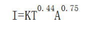
According to the calculation formula of mass, M = ρ× V (volume) = ρ× S (area) × T (thickness), knowing the weight of copper foil divided by the density and area of copper is the thickness of copper foil!
As we know from the above, 1oz = t × 929.0304cm2 × 8.9g/ cm3=28.35g
Therefore, t = 28.35 ÷ 929.0304 ÷ 8.9cm ≈ 0.0034287cm = 34.287um ≈ 34.287 ÷ 25.4mil ≈ 1.35mil
Therefore, the thickness of 1oz copper foil is about 35um or 1.35mil.
Copper thickness 1 Oz (0.035mm) copper thickness 1.5oz (0.05mm) copper thickness 2.5mm OZ(0.07mm)
Relationship between PCB line width and current:
First calculate the cross-sectional area of the track. The copper foil thickness of most PCBs is 35um (if you are not sure, ask the PCB manufacturer). Multiply it by the line width is the cross-sectional area. Pay attention to converting it into square millimeters. There is an empirical value of current density, which is 15 ~ 25 A / mm2. Call it the upper cross-sectional area to get the flow capacity.
The calculation of PCB current carrying capacity has been lack of authoritative technical methods and formulas. Experienced CAD engineers can make more accurate judgment by relying on personal experience. But for CAD novices, it can be said that they have encountered a difficult problem.
The current carrying capacity of PCB depends on the following factors: line width, line thickness (copper foil thickness) and allowable temperature rise. As we all know, the wider the PCB wiring, the greater the current carrying capacity. Here, please tell me: assuming that the wiring of 10mil can withstand 1A under the same conditions, what current can the wiring of 50mil withstand, 5A? The answer is naturally No. Please see the following data from international authorities:
The unit of line width is: inch (inch = 25.4 millimetres mm) 1 oz. copper = 35 microns thick, 2 oz. = 70 microns thick, 1 oz = 0.035mm 1mil= 10-3inch.
The voltage drop caused by the line resistance caused by the length of the conductor must also be considered in the experiment. The tin used in process welding is only to increase the current capacity, but it is difficult to control the volume of tin. 1oz copper, 1mm wide, generally used as 1 – 3A galvanometer, depending on your line length and voltage drop requirements.
The maximum current value should refer to the maximum allowable value under the temperature rise limit, and the fusing value is the value when the temperature rise reaches the melting point of copper. Eg. 50mil 1oz temperature rise 1060 degrees (i.e. copper melting point), current is 22.8a


