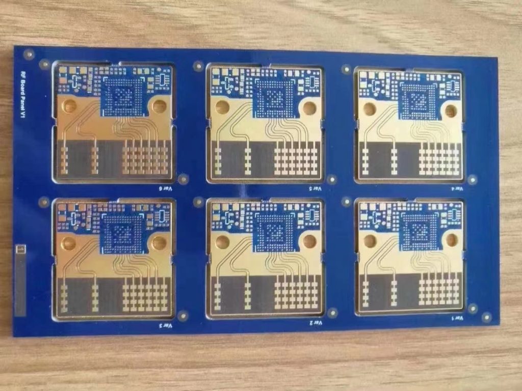
PCB ENIG (Electroless Nickel Immersion Gold) and PCB gold plating are two common surface finish techniques used in the fabrication of printed circuit boards (PCBs). Here are the key differences between ENIG and gold plating:

ENIG (Electroless Nickel Immersion Gold):
- Composition:
- ENIG involves a two-step process. First, a thin layer of nickel is deposited onto the exposed copper surface through a chemical reaction (electroless deposition). Then, a layer of gold is applied through immersion in a gold solution.
- The gold layer is typically quite thin, usually around 1-2 microinches (25-50 micro-microns) thick.
- Corrosion Resistance:
- ENIG offers excellent corrosion resistance due to the protective nickel layer. It is well-suited for applications that require long-term reliability and resistance to harsh environments.
- Solderability:
- ENIG provides good solderability, making it suitable for surface-mount technology (SMT) and fine-pitch components. The gold layer is solderable, and the nickel layer acts as a barrier to prevent the copper from oxidizing.
- Flat Surface Finish:
- ENIG produces a flat and smooth surface finish, which is beneficial for fine-pitch components and for achieving uniform solder paste distribution during assembly.
Gold Plating:
- Composition:
- Gold plating is a one-step process where a layer of gold is directly applied to the exposed copper surface. The thickness of the gold layer can vary based on the application but is typically thicker than that of ENIG.
- Corrosion Resistance:
- Gold plating also provides good corrosion resistance, although it may not be as robust as ENIG due to the absence of a nickel barrier layer.
- Solderability:
- Gold is inherently solderable, which makes gold-plated surfaces suitable for soldering. However, the solderability may degrade over time due to the migration of gold atoms to the solder joint.
- Contact Reliability:
- Gold plating is often used in applications where contact reliability is critical, such as connectors and switches, because gold does not tarnish or corrode, ensuring consistent electrical performance.
In summary, ENIG combines the corrosion resistance of nickel with the solderability of gold and is well-suited for applications with high-reliability and fine-pitch requirements. Gold plating, on the other hand, is used when solderability and contact reliability are paramount, and the corrosion resistance of gold is sufficient. The choice between these surface finishes depends on the specific requirements of the PCB and the intended application.

