
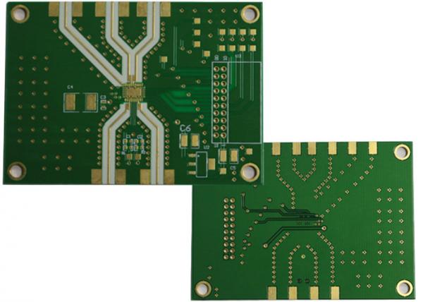
High frequency PCB wiring design principle
1. Minimize logical fan out, preferably with only one load.
2. Avoid using a thorough hole between the output of the high-speed signal line and the receiving end as far as possible to avoid the cross of the pin figure. Clock signal lines, in particular, require special attention.
3. Adjacent signal lines should be perpendicular to each other to avoid turning at right angles.
4. Load resistors connected in parallel shall be as close to the receiving end as possible.
5. In order to ensure minimum reflection, all open routes (or lines without end match) must meet the relevant mathematical formula
6. When the opening length of the high frequency printed circuit board exceeds the above value, the series damping resistor shall be used and the series terminal resistance shall be connected to the pin of the output terminal as far as possible.
7. To ensure that analog and digital circuits are separated, the high frequency PCB AGND and DGND must be connected together by an inductor or magnetic bead and as close to A/D converter as possible.
8. Ensure sufficient decoupling of power supply.
9. It is best to use surface mounted resistance and capacitance.


