
The design of electronic products is a complex and multifaceted process that involves several key stages, from conceptualization to the introduction of the Printed Circuit Board (PCB). Here is an overview of the basic process of electronic product design, with a focus on PCB introduction:
1. Conceptualization:
2. Feasibility Study:
3. Schematic Design:
4. Component Selection:
5. PCB Design:
6. PCB Prototyping:
7. Firmware/Software Development:
8. Testing and Iteration:
9. Regulatory Compliance and Certification:
10. Production Preparation:
11. Mass Production:
12. Quality Control:
13. Packaging and Distribution:
14. Post-Market Support:
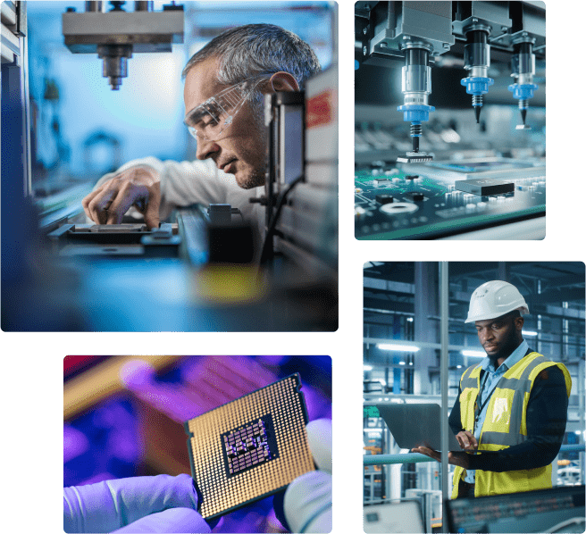
The Printed Circuit Board (PCB) is a central component in this process. It acts as the physical platform for the electronic circuit, translating the schematic into a tangible layout. PCB design encompasses considerations such as component placement, trace routing, and signal integrity. A well-designed PCB is pivotal to the functionality and reliability of the electronic product.
In summary, the design of electronic products involves a comprehensive process with multiple phases, from the initial concept to post-market support. PCB design is a pivotal step in this process, enabling the physical realization of the electronic circuit and playing a crucial role in the product’s functionality and performance.
Printed circuit boards (PCBs) refer to boards that are processed into certain sizes on the basis of insulating substrates. At least one conductive pattern and all designed holes (such as component holes, mechanical mounting holes and metallized holes) are arranged on it to realize electrical interconnection between components.
Printed circuit boards usually play four roles in electronic equipment.
(1) Provide necessary mechanical support for various components in the circuit.
(2) Provide electrical connection of circuit to realize wiring or electrical insulation between various components such as integrated circuits.
(3) Provide the electrical characteristics required by the circuit, such as characteristic impedance.
(4) Each component installed on the board is marked with marking symbols for easy installation, inspection and debugging.


