However, if these probes are allowed to directly contact the electronic components or their solder pins on the board, it is likely to crush some electronic components, which is just the opposite.
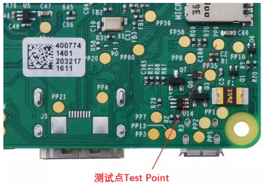
So smart engineers invented the “test point”, which leads out a pair of circular dots at both ends of the part. There is no solver mask on it, so that the probe for testing can contact these dots instead of directly contacting the electronic components to be measured.
In the early days of traditional plug-in (DIP) on the circuit board, it was true that the solder pins of parts were used as test points, because the solder pins of traditional parts were strong enough and not afraid of pinpricking, but there were often misjudgments of poor contact of probes.
Because the general electronic components after the wave soldering or SMT eat tin, in its solder surface will usually form a layer of solder paste flux residual film, this layer of film impedance is very high, often cause poor contact of the probe.
So at that time, we often see the production line test operators, often blowing desperately with the air gun, or wiping the places that need to be tested with alcohol.
In fact, after wave soldering test point will also have the problem of poor contact probe. Later, after the popularity of SMT, the situation of test misjudgment has been greatly improved, and the application of test points has been greatly entrusted with a heavy task.
Because the components assembled by PCB are usually very fragile and can’t bear the direct contact pressure of the test probe, the use of test points can not make the probe directly contact the components and their solder pins, which not only protects the components from damage, but also indirectly greatly improves the reliability of the test, because there are fewer misjudgments.
However, with the development of science and technology, the size of circuit board is getting smaller and smaller. It’s hard to squeeze so many electronic components on a small circuit board. Therefore, the problem of test point occupying circuit board space is often a tug of war between
PCB design end and
PCB manufacturing end.
The appearance of the test point is usually round, because the probe is also round, which is better for production, and it is easier to make the adjacent probes closer, so as to increase the needle planting density of the needle bed.
For example, the minimum diameter of the probe has a certain limit, and the needle with too small diameter is easy to break and damage.
There is also a certain limit to the distance between pins, because each pin has to come out of a hole, and the back end of each pin has to be welded with a flat cable.
If the adjacent holes are too small, in addition to the problem of contact short circuit between pins, the interference of flat cable is also a big problem.
Some high-resolution devices can not be planted next to the needle. If the probe is too close to the high component, there will be a risk of damage caused by collision with the high component. In addition, due to the high component, it is usually necessary to open a hole on the needle bed seat of the test fixture to avoid it, which indirectly results in the failure of needle implantation. It is more and more difficult to hold all the test points of components on the circuit board.
As the board becomes smaller and smaller, the number of test points has been discussed repeatedly. Now there are some methods to reduce the number of test points, such as net test, test jet, boundary scan, JTAG, etc; There are also other test methods that want to replace the original needle bed test, such as AOI and X-ray, but at present, each test can not replace ICT 100%.
As for the needle planting ability of ICT, we should ask the fixture manufacturer, that is, the minimum diameter of the test point and the minimum distance between the adjacent test points. Generally, there will be a desired minimum value and the minimum value that the ability can reach. However, PCB manufacturers with large scale will require that the distance between the minimum test point and the minimum test point can not exceed how many points, otherwise the fixture will be easily damaged.