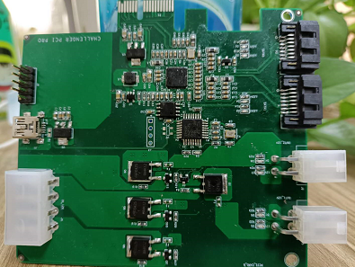
There are PCB prototype boards and Complex PCB boards. It is unnecessary to say that the prototype of a simple PCB is easy, but if it is a complex PCB prototype, you should be careful. If you do not use relevant testing tools to detect PCB prototype design, if there is a problem, it will be late to find out when the PCB is ready. Therefore, we must make full preparation before manufacturing the prototype.

1. Making physical outline
The closed physical outline is a basic platform for the future component layout and PCB prototype. We must pay attention to the accuracy. Moreover, it is better to use arc at the corner, which can not only avoid being scratched by sharp corners, but also reduce the stress effect.
2. The introduction of electronic components and networks, and the layout of components
In the design of PCB prototype, electronic components and network should be introduced into the designed outline carefully, including the encapsulation form of electronic components and network problems of electronic components. Because of the contrast, it is not easy to have problems. In PCB prototype, the layout of electronic components and wiring has a great impact on product life, stability, electromagnetic compatibility, which should be paid special attention to. Generally speaking, there should be the following principles: placement order, attention to heat dissipation.
3. PCB design, wiring and adjustment
In PCB design and wiring, it is best to pay attention to the requirements of processing parameters, or to reliable PCB prototype manufacturers, the defective rate will be greatly reduced. After the completion of PCB design and wiring, it is necessary to make some adjustments to the text, individual electronic components and wiring, and copper pour (this work should not be too early, otherwise it will affect the speed and bring trouble to PCB design and wiring), which is also for the convenience of production, debugging and maintenance.
4. Check the network
Sometimes because of mis operation or negligence, the network relationship of the
PCB layout is different from the schematic diagram, so it is necessary to check. Therefore, the layout should be checked first and then follow-up work.

