PCB layout is PCB design.PCB design needs to be realized by computer aided design. The commonly used design software in the industry is cadence Allegro, pads, Altium designer.
Conventional PCB design includes several steps, such as database building, network adjustment table, layout, wiring, file output, etc., but the conventional PCB design process is far from meeting the increasingly complex high-speed PCB design requirements. Because Si simulation, PI simulation, EMC design, single board process and so on need to be closely integrated into the design process. At the same time, in order to achieve quality control, the review link should be added at each node. The actual PCB design process is much more complex.
Electronic components commonly used in
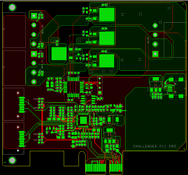
PCB layout.
Especially when drawing the schematic diagram with pads9.3 or Allegro 16.3, it is necessary to understand the English of common electronic components. Generally, the first three English letters of a part are used to replace a part, such as res for resistance, cap for capacitance and ind for inductance. A part is listed below.
Voltage
Current
Ohm
Volt
Ampere
Watt
Circuit
Circuit element
Resistance
Resistor
Inductance
Inductor
Capacitance
Capacitor
Ohm’s law
Kirchhoff’s law
Kirchhoff’s voltage law (KVL)
Kirchhoff’s current law (KCl)
Loop
Network
Passive two terminal network
Active two terminal network


