
The goal of PCB design is to be smaller, faster and cheaper. Because the interconnection point is the weakest link in the circuit chain, the electromagnetic property of the interconnection point is the main problem in RF design. It is necessary to investigate each interconnection point and solve the existing problems. The interconnection of PCB system includes chip to circuit board, PCB intra-board interconnection and signal input/output between PCB and external devices. This paper mainly introduces the practical skills of PCB board interconnection for high frequency PCB design. I believe that the understanding of this paper will bring convenience to PCB design in the future.
In the design of PCB, the interconnection between chip and PCB is very important for the design. However, the main problem of interconnection between chips and PCBs is that the high interconnection density will lead to the basic structure of PCB materials as a limiting factor for the growth of interconnection density. This paper shares the practical skills of high frequency PCB design. In terms of high-frequency applications, the techniques for designing high-frequency PCB for PCB intra board interconnection are as follows:
1. The corner of transmission line should adopt 45-degree angle to reduce the return loss.
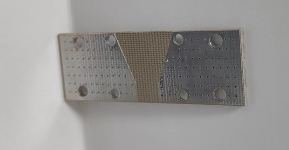
2. High performance dielectric circuit boards whose dielectric constant values are strictly controlled by the number of layers should be adopted. This method is helpful for effective simulation calculation of electromagnetic field between insulating material and adjacent wiring.
3. The PCB design specifications for high precision etching should be stipulated. Consider setting the total line width error of +/-0.0007 inches, managing the undercut and cross section of the wiring shape, and specifying the plating conditions for the side wall of the wiring. Overall management of wiring (conductor) geometry and coating surface is very important for solving skin effect problems related to microwave frequency and realizing these specifications.
4. There are tap inductance and parasitic effect in the protruding pin lead, so the components with lead should be avoided. In high frequency environment, it is better to install SMD components on the surface.
5. For signal through-hole, it is necessary to avoid the use of through-hole processing (pth) technology on the sensitive board, because this technology will lead to lead inductance at the through-hole. If a through hole on a 20-layer board is used to connect layers 1 to 3, there are 4 to 19 layers of lead inductance. Buried blind holes or back drills should be used.
6. Provide abundant grounding layer. The grounding layers should be connected by moulding holes to prevent the influence of 3-D electromagnetic field on the circuit board.
7. To choose non-electrolytic nickel plating or immersion gold plating process, do not use HASL method for electroplating. This kind of plating surface can provide better skin effect for high frequency current.
In addition, this high weldable coating requires fewer leads, which helps to reduce environmental pollution.
8. The solder paste flow can be prevented by the solder barrier layer.
However, due to the uncertainty of thickness and dielectric constant, covering the whole plate surface with solder-resistant materials will lead to the change of circuit performance in microstrip design. Solder dam is usually used as the welding resistance layer.
As a high frequency PCB manufacturer, PCBSky sells high frequency PCB abroad all year round. Welcome to consult!


