
Why the bare copper pad on the side of QFN device and pad on the back side of SMT welding do not climb tin or the height of tin climbing can not meet the standard requirements in IPC, which is a knotty and headache problem. How to solve this problem, today we will talk about the potential hazards of QFN side pad that does not climb tin, which brings about contact false soldering and unstable function test.
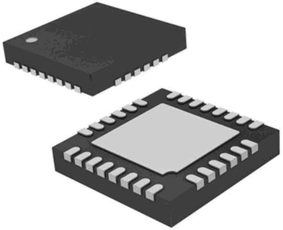
With the development of electronic industry, PCB wiring is becoming more and more compact, and more and more QFN devices are selected. Because QFN devices are small in size, light in weight and excellent in electrical and thermal properties, this kind of package is especially suitable for any product application that requires size, weight and performance. Because QFN package does not have gull wing like lead as traditional SOIC and TSOP packages do It can provide excellent electrical performance because of the short conductive path between the internal pin and the pad, the low self inductance coefficient and the wiring resistance in the package. Compared with the traditional 28 pin PLCC package, the area (5mm × 5mm) of 32 pin QFN is reduced by 84%, the thickness (0.9mm) is reduced by 80%, the weight (0.06g) is reduced by 95%, and the parasitic effect of electronic package is also increased by 50%. Therefore, it is very suitable for high-density printed circuit boards of mobile phones, digital cameras, PDAs and other portable small electronic devices.


