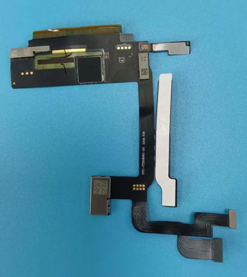
Flexible circuit board manufacturing involves several steps to create a flexible printed circuit board (PCB) tailored to a specific application. Here’s a general outline of the process:
- Design and Prototyping:
- Define the circuit’s schematic and layout using PCB design software.
- Create a prototype to test the circuit’s functionality and ensure it meets the requirements.
- Material Selection:
- Choose suitable materials, such as flexible substrate material (e.g., polyimide), copper foil, and adhesive layers, based on the application’s requirements.
- Substrate Preparation:
- Clean and prepare the flexible substrate material, ensuring it is free from contaminants and defects.
- Copper Cladding:
- Apply a thin layer of copper foil to both sides of the substrate. This copper will serve as the conductive traces.
- Lamination:
- Stack and laminate the layers together, including the substrate, copper foils, and adhesive layers. Apply heat and pressure to bond them.
- Photoresist Application:
- Apply a photoresist material to the copper-clad substrate. This photoresist will be used to define the circuit pattern.
- Exposure and Development:
- Use a UV light source and a photomask to expose the photoresist to the desired circuit pattern.
- Develop the exposed photoresist to reveal the copper traces pattern.
- Etching:
- Submerge the board in an etchant solution (usually an acidic solution) to remove the unwanted copper, leaving behind the circuit traces.
- Cleaning:
- Thoroughly clean the board to remove any remaining photoresist and etchant residue.
- Surface Finish:
- Apply a surface finish to protect the exposed copper traces and enhance their solderability. Common finishes include gold plating, HASL (Hot Air Solder Leveling), or ENIG (Electroless Nickel Immersion Gold).
- Solder Mask Application:
- Apply a solder mask over the entire board, leaving openings for solder pads and vias.
- Silkscreen Printing:
- Add component labels, reference designators, and other necessary markings to the board using silkscreen printing.
- Component Assembly:
- Attach components to the board using pick-and-place machines and solder reflow ovens. This step may involve both surface-mount and through-hole components.
- Testing and Inspection:
- Conduct electrical testing to ensure the circuit functions correctly.
- Inspect the board for any defects or manufacturing errors.
- Cutting and Shaping:
- Cut the flexible PCB into the desired shape and size, following the design specifications.
- Final Inspection:
- Conduct a final inspection to verify that the board meets all quality and performance criteria.
- Packaging and Delivery:
- Package the flexible circuit boards appropriately for shipping or assembly into the final product.
Keep in mind that the specific details of the manufacturing process may vary depending on the complexity of the design, the materials used, and the equipment available at the manufacturing facility. It’s important to follow industry standards and quality control practices throughout the process to ensure reliable and consistent results.