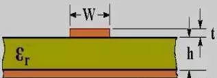
Answer: the quality of transmission lines for high-speed transmission and high-frequency signal transmission is much stricter than that of transmission wires. It is no longer "open / short circuit" test pass, or notch, burr does not exceed 20% of the line width. It must be required to measure the characteristic impedance value, and the impedance should be controlled within the tolerance, otherwise, it is only scrapped and cannot be reworked.
Control reason of characteristic impedance value:
Reason 1
When the electronic equipment (computer, communication machine) is operating, the signal sent by the driver will be sent to the receiver through
PCB transmission line. When the signal is transmitted in the signal line of the printed circuit board, the characteristic impedance value Z0 must match the "electronic impedance" of the head and tail components, so that the "energy" in the signal can be transmitted completely.
Reason 2
Once the quality of printed circuit board is poor and Z0 exceeds the tolerance, the transmitted signal will have problems such as reflection, departure, attention or delay, and in serious cases, the wrong signal will be transmitted and the machine will crash.
Reason 3
Strict selection of plates and control of the production process, the Z0 on the multilayer board can meet the specifications required by customers. The higher the electronic impedance is, the faster the transmission speed will be. Therefore, the Z0 of PCB must be improved to meet the requirements of matching components. Only when Z0 is qualified, can it be regarded as the qualified product required by high-speed or high-frequency signals.
More experience:
1. Digital signals above 50 MHz need to control impedance
2. RF signal needs to control impedance
3. Analog signal does not control impedance generally