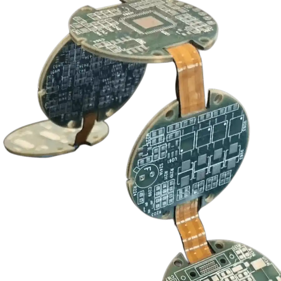
Manufacturing rigid flexible circuit boards (rigid flex PCBs) combines the features of both rigid and flexible PCBs. This process involves intricate steps to create a board that can be folded or bent to fit the shape of a device while maintaining rigidity in certain areas. Below is a comprehensive manufacturing process for rigid flex PCBs:
Design and Prototyping:
Develop the circuit schematic and layout using PCB design software.
Create prototypes to test the functionality and verify that the rigid-flex design meets the requirements.
Material Selection:
Choose appropriate materials, including rigid and flexible substrates, copper foils, and adhesive materials, based on the project’s needs and specifications.
Rigid and Flexible Substrate Preparation:
Clean and prepare the rigid and flexible substrates to ensure they are free from contaminants and defects.
Copper Cladding:
Apply copper foils to both the rigid and flexible substrates to create conductive layers.
Lamination:
Stack and laminate the rigid and flexible layers together using adhesive materials.
Apply heat and pressure to bond the layers into a single structure.
Drilling and Plating:
Drill holes for vias and component leads through the entire stack.
Plate the holes with conductive material to create the interconnections between layers.
Copper Etching:
Apply a photoresist layer and expose it to UV light through a photomask to define the copper traces.
Develop and etch away the unwanted copper to reveal the circuit pattern.
Cleaning:
Thoroughly clean the board to remove any remaining photoresist and etchant residue.
Surface Finish:
Apply a surface finish to protect the exposed copper traces and enhance their solderability. Common finishes include ENIG, HASL, or OSP.
Solder Mask Application:
Apply solder mask over the entire board, leaving openings for solder pads, vias, and flexible regions.
Silkscreen Printing:
Add component labels, reference designators, and other markings to the board using silkscreen printing.
Component Assembly:
Attach components to the rigid areas of the board using pick-and-place machines and solder reflow ovens.
Ensure proper anchoring and secure attachment of components in the flexible areas.
Testing and Inspection:
Conduct electrical testing to ensure the circuit functions correctly.
Inspect the board for defects or manufacturing errors.
Cutting and Shaping:
Cut and shape the rigid-flex PCB to match the desired form and fit within the device or enclosure.
Final Inspection:
Perform a final inspection to verify that the board meets all quality and performance standards.
Packaging and Delivery:
Package the rigid-flex PCBs appropriately for shipping or assembly into the final product.
Environmental Considerations:
Ensure that the rigid-flex PCB design and materials can withstand the intended environmental conditions, such as temperature extremes, humidity, and exposure to chemicals or moisture.
Documentation:
Maintain comprehensive documentation throughout the manufacturing process, including design files, material specifications, and quality control records.
Quality Control:
Implement a robust quality control process to identify and address any manufacturing defects promptly.
Prototyping and Testing:
Create prototypes to test and validate the design before full-scale production.
Compliance and Standards:
Ensure that the rigid-flex PCB complies with relevant industry standards and certifications, especially if the application requires compliance.
Rigid-flex PCB manufacturing is a complex and specialized process, so it’s important to work with experienced manufacturers who have expertise in producing high-quality rigid-flex circuits that meet your specific project requirements. Effective communication and collaboration with your PCB manufacturer are crucial to address any unique concerns or design considerations.