In the dynamic landscape of modern electronics, innovation paves the way for smaller, smarter, and more powerful devices. High-Density Interconnect (HDI) PCB technology has emerged as a driving force behind this evolution, enabling the creation of compact yet high-performance electronic devices. In this article, we will explore the world of HDI PCBs, understanding their significance, benefits, applications, and how they are shaping the future of electronics.
Understanding HDI PCBs
High-Density Interconnect (HDI) PCBs represent a breakthrough in PCB design and manufacturing, achieving a higher level of miniaturization and complexity compared to traditional PCBs. HDI PCBs are characterized by their dense arrangement of components, finer traces, and multiple layers of interconnected circuitry. These advancements allow for increased functionality and performance within a smaller form factor.
Key Attributes of HDI PCBs
- Layer Density: HDI PCBs consist of multiple layers, often ranging from 4 to 10 layers or more, densely packed to accommodate complex circuitry in a limited space.
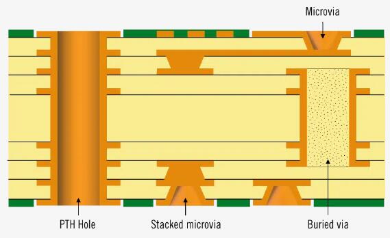
- Microvias and Fine Lines: Microvias, small drilled holes with diameters as fine as 0.1mm, enable connections between different layers. Fine traces allow for intricate routing and high-speed signal transmission.
- Advanced Materials: HDI PCBs often utilize advanced materials with excellent electrical properties, enabling higher frequency operation and signal integrity.
- Component Placement: HDI technology enables tighter component placement, reducing signal delay and optimizing signal propagation.
Benefits of HDI PCBs
- Miniaturization: The primary advantage of HDI PCBs is their ability to achieve significant miniaturization, making them ideal for compact devices where space is a premium.
- Increased Functionality: HDI technology allows for more components to be placed within a smaller area, leading to enhanced device functionality and capabilities.
- High-Speed Performance: The finer traces and microvias in HDI PCBs enable high-speed signal transmission, reducing signal loss and distortion.
- Improved Signal Integrity: HDI PCBs offer better control over impedance, reducing signal reflections and maintaining signal integrity, crucial for high-frequency applications.
- Reduced Electromagnetic Interference (EMI): The compact design of HDI PCBs and the ability to manage signal routing efficiently contribute to reduced EMI, enhancing overall performance.
Types of HDI PCBs
- 1+N+1 HDI PCB: This type includes a single build-up layer with two layers of high-density interconnects on either side of the core layer. It’s suitable for applications requiring moderate component density.
- 2+N+2 HDI PCB: With two build-up layers and two layers of high-density interconnects on either side of the core, this type offers higher component density and greater design flexibility.
- 3+N+3 HDI PCB: The 3+N+3 configuration includes three build-up layers and three layers of high-density interconnects on each side of the core. It’s suitable for the most complex and compact PCB designs.
Applications of HDI PCBs
- Mobile Devices: HDI PCBs are widely used in smartphones, tablets, and wearables, where space constraints demand compact yet high-performance circuitry.
- Consumer Electronics: Compact consumer electronics like digital cameras, gaming consoles, and smart home devices benefit from the miniaturization and improved performance offered by HDI PCBs.
- Medical Devices: In medical devices such as implantable devices, diagnostic equipment, and monitoring systems, HDI PCBs play a crucial role in enabling advanced functionality within limited space.
- Aerospace and Defense: In avionics systems, radar equipment, and communication devices, HDI PCBs contribute to lightweight yet robust electronics for critical applications.
- Automotive Electronics: The automotive industry leverages HDI PCBs for advanced driver-assistance systems (ADAS), infotainment systems, and engine control units (ECUs).
Navigating the Challenges of HDI PCBs
While HDI PCBs offer numerous benefits, they also present challenges that need to be managed effectively:
- Manufacturing Complexity: The intricate design and multiple layers of HDI PCBs require advanced manufacturing processes and specialized equipment.
- Design Constraints: The miniaturization of components and traces demands meticulous attention to design rules, material selection, and impedance control.
- Cost Considerations: The increased complexity of HDI PCBs can lead to higher manufacturing costs compared to traditional PCBs.
- Testing and Inspection: The compact nature of HDI PCBs can make testing and inspection more challenging, necessitating advanced techniques and equipment.
Choosing the Right HDI PCB Solution
When considering HDI PCB technology for your project, several factors come into play:
- Design Expertise: Collaborate with a PCB manufacturer or designer experienced in HDI technology to ensure proper design, impedance control, and manufacturability.
- Material Selection: Choose advanced materials that offer the necessary electrical properties for your application, while also considering manufacturing constraints.
- Manufacturing Capability: Partner with a manufacturer equipped with the latest technology and expertise to handle the complexities of HDI PCB fabrication.
- Cost-Effectiveness: Balance the benefits of HDI PCBs with the associated costs, ensuring that the technology aligns with your project’s budget and goals.
HDI PCB technology has revolutionized the electronics industry by enabling the creation of smaller, more powerful, and more complex devices. The benefits of miniaturization, increased functionality, high-speed performance, and improved signal integrity make HDI PCBs indispensable in applications ranging from mobile devices to aerospace systems. While challenges such as manufacturing complexity and cost considerations exist, they can be effectively managed through collaboration with experienced partners and careful design practices. As technology continues to advance, HDI PCBs will remain at the forefront of innovation, driving the creation of cutting-edge electronic devices that shape our interconnected world.